This thread has been locked.

If you have a related question, please click the "Ask a related question" button in the top right corner. The newly created question will be automatically linked to this question.

TPSM82813: layout of via

Part Number: TPSM82813

Hi,

I found the post below.

https://e2e.ti.com/support/power-management-group/power-management/f/power-management-forum/1125125/tpsm82813-vout-side-of-the-piggybacked-inductor/4174857?tisearch=e2e-quicksearch&keymatch=TPSM82813%20via#4174857

I was wondering if you could answer some questions about via.

1.Would it be OK to place the via next to the pad as shown in the figure below?

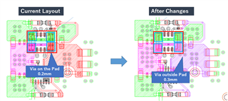
2.If the via is placed next to the pad, the FB loop would be longer, but would it be OK?

3.Would it be OK to place the via on the pad and change the via diameter from 0.2 mm to 0.15 mm or 0.1 mm?

Best Regards,

Nishie

  • Hi Nishie,

    1. It is alright to place the vias next to the pad.
    2. I don't see why the FB loop gets longer. Could you illustrate why it gets longer?
    3. We haven't done experiments with non-pre-plugged vias of different quantities and diameters on the pads to determine if there would be soldering problem. The recommendation would be to pre-plug the vias placed on the pads.

    Best regards,

    Varun

  • Hi Varun-san,

    Thank you for your reply.

    1. I understand.

    2. The customer makes a FB loop on the back through the via like EVM.
        So moving the via lengthens the loop.
        Customers are concerned about whether this has a significant impact on the output voltage.

        Fig.5-5

     www.ti.com/.../sluuc44a.pdf

    3. I will explain to customers that I did not conduct experiments.
        By the way, when I mounted it with the via on the pad having a diameter of 0.2 mm, the solder was absorbed by the via and the mounting failure occurred.
        For this reason, I thought about reducing the via diameter.

    Best Regards,

    Nishie

  • Hi Nishie-san,

    Thanks. The lengthening of the FB loop should be marginal and not cause a regulation issue.

    Best regards,

    Varun

  • Hi Varun-san,

    I have received some additional questions from clients.
    I would appreciate it if you could answer them.

    1.Is there any change in characteristics with the change in impedance between the pad-on-via and placing the via next to the pad?

    2.Have you ever done an evaluation on a board with the via placed next to the pad and no via on the pad?

    3. Have you ever done an evaluation on a board with a via plug?

    4. If there are any conditions for a via plug, could you tell me?

    Best Regards,

    Nishie

  • Hi Nishie-san,

    For this device, we have only evaluated boards with vias in the pads. The vias (0.2mm hole diameter) on the pads were pre-plugged. However I don't expect a significant change in performance except for thermals by placing the vias just outside the pads. The vias in the pads mainly help improve thermal performance of the module. 

    Could you find out the steady-state load and max load (as well as time duration at max load) the customer expects to operate at?

    Best regards,

    Varun 

  • Hi Varun-san,

    Thank you for your support.

    Am I correct in understanding that all of the device characteristics listed in the data sheet were evaluated with the via plugged?

    Also, the customer load conditions are as follows:
    Steady load = 0.8A
    max load = 1.2A

    From this information, is it correct to understand that you will place the via next to the pad and check if there is no problem?

    Best Regards,

    Nishie

  • Hi Nishie-san,

    Yes you are correct, all the datasheet parameters are measured with the EVMs that had plugged vias in the pads.

    What is the max ambient temperature of the application? The customer load currents mentioned are not that high and vias in pads may not be required if max ambient temp is not high. The important thing is to estimate the junction to ambient thermal resistance of the customer board to estimate if the max junction temperature of 125C is exceeded or not. You can refer to the following app notes about thermal resistance. 1. https://www.ti.com/lit/ml/snva848a/snva848a.pdf 2. https://www.ti.com/lit/ml/slvaei9/slvaei9.pdf

    Is cost the reason why the customer is not able to use plugged vias?

    We wouldn't be able to support a new EVM design with the vias outside the pads. 

    Best regards,

    Varun

  • Hi Varun-san,

    Thank you for your reply.

    1. What is the max ambient temperature of the application? 

    ->max ambient temperature is 70℃.

    2. Is cost the reason why the customer is not able to use plugged vias?

    -> Yes. Customers are concerned about cost.
    Therefore, we are considering placing a via next to the pad rather than pre-plugged.

    Best Regards,

    Nishie