This thread has been locked.

If you have a related question, please click the "Ask a related question" button in the top right corner. The newly created question will be automatically linked to this question.

LMG3410R070: switch off power loss abnormal

Part Number: LMG3410R070
Other Parts Discussed in Thread: TIDA-010062,

Hi,

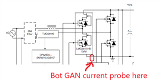
We are developing totem pole bridgeless PFC which based on TIDA-010062. The GAN just use LMG3410R070 demo board LMG3410-HBEVM for high frequency switch. In our test, we found that PFC efficiency is not high. The main loss may be GAN. We use DC input and set PWM duty cycle of fixed 0.2 or 0.5. When Vbus voltage raised to high voltage, the bot GAN temperature become higher than top GAN. Our analysis is Bot GAN switch off power loss is high. Below is waveform of Bot GAN, please help to check.

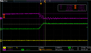
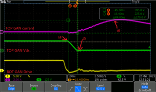
The waveform is BOT GAN driver, Vds and current with Zoom In.

Input is 100V DC and output VBUS is 125V with 1A load. Duty is fixed of 0.2.

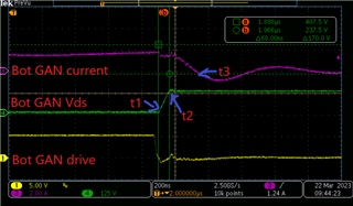
From t1, GAN switch off, current drive Coss so that Vds increased to 125V. 

Question 1: The rise time of Vds is about 68ns, which seem too slow. According 2A current to drive Coss of about 150pf to 125V. The time should be C*U/I= 9.4ns. Why here is 68ns?

Question 2: From t2 to t3 of about 200ns, although Vds is 125v and GAN switch off, but there still have current draw from D to S. The deadtime is 100ns. So 32ns after t2, top Gan already swithed on. But current still pass through Bot GAN, which act like reverse recovery but in fact GAN should no this feature. This U*I involve much higher power loss. Do you know what happened at t2 to t3?

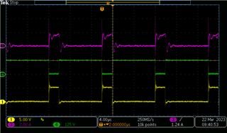
From below waveform of Top GAN, we can see current is not flow to TOP GAN immediately after Bot GAN switching off. From t4 to t5, TOP GAN in the Third Quadrant operation. But current maily not through TOP GAN. After t5, TOP GAN was completely switched on, but current still raised slowly till t6 then all current though TOP GAN.  The Delta of current from t5 to t6 is current through BOT GAN of t2 to t3.

Please help to check the waveforms, thanks.


  • Hello,

    How fast is the current probe being used? The first scope shot seems very strange. DC current probes are generally much slower than voltage probes, and the current graph seems slow. Additionally, there's a weird low frequency oscillation in the current graph that I can't explain.

    To answer your questions:

    1. That is slower than I'd expect.

    2. I'm not sure how to explain this. Current must either flow through the junction or through the VDS capacitor. Current can't be flowing through the junction because the FET is off. Current can't be flowing through the VDS cap because VDS does not change after T2. For this reason, I'm wondering if the current probe is accurate over the short time periods.

    Questions for you:

    1. What is the RDRV resistor value?

    2. What model current probe is being used? What is the bandwidth and rise time?

    Thanks,

    Travis

  • Hi,

    The turnoff slew is denpends on the turnoff current, which will charge the Coss of GaN. This couldn't be adjusted by the drving strength, and won't influence your efficiency.

    Your low side GaN is hotter in positive DC input, this is because the Eoss energy of both high and low side are consumed ONLY on low side GaN, when it is turnning on. This is normal.

    Question1 is good, this maybe the cause of low efficiency. But you need to find out where is the extra Coss exsiting, we can't help you without knowing your design and setup.

    for your question2, Have you exculde the current of decoupling Cap on the daughter card? This current maybe the resonant between the decouping cap and the parasitic L on your board.

  • Hi, Travis

    1. RDRV is 15k

    2. the current probe is Textronix TCP0030A. Bandwith >120MHZ and rise time <2.92ns.

    Best Regards

  • Hello Desheng,

    You are right, the current of t2 to t3 is caused by resonant between decoupling cap on daughter board and L on Monther board. After removing all caps in daughter board. The current went to 0 after VDS raising to 125V. Does the resonant impact efficiency?

    For the Coss, board layout coupling will add some capacitor. After I connecting GAN demo board SW pin directly to Inductor, the switch off time improved from 68ns to 49ns.  From above picture, the Coss is about 300pF which twice than datasheet.

    Best Regards,