This thread has been locked.

If you have a related question, please click the "Ask a related question" button in the top right corner. The newly created question will be automatically linked to this question.

UCC28180: Current sense signal

Part Number: UCC28180

Hello,

I am trying to test a control card with UCC28180, but before testing it with the High Power plant/ baseboard, I want to test the controller card individually to check if it gives desired gate output.

For 65kHz operation,

Input of 5V is given to Vsense (pin6)

Providing 15V to Vcc(pin7)

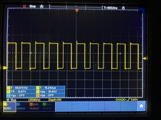
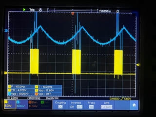
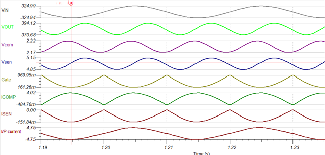
For Isense(pin3) :  Through Function generator, I am planning to input a waveform that will be similar to a current sense waveform from a plant / baseboard.

But I cannot find any snapshots of the actual resulting current sense signal(going into pin3) in any of the PFC EVM board documentation to be used as a reference.

Can you please provide the same.

Regards,

.

  • Hi,

    Thank you for the query on UCC28180. I do not have the waveforms handy but have simulated a typical one for you.

    The  ISENSE pin voltage is from sense resistor and it will be scaled by the current from through it. 

    IL below shows current in inductor and D4 voltage is the voltage at ISENSE pin (it will be multiplied by -2.5 gain internally)

    Regards,

    Harish

  • Hello,

    As mentioned above I have provided signals to UCC28180 controller card to check the gate output waveform as below:

    Vcc = 15V, Vout = 5V(after stepping down 400V), Isense = -200mV peak. 

    However, looks like showing discontinuous behavior, the switching is only occurring at certain intervals. (which is not even happening near the peak of Isense wave)


    (Blue: Isense || Yellow: Output Gate signal)

    Could you please explain what might be the issue here?

    Regards,

    Sajal

  • Hi Sajal,

    Thank you for the query.

    I would recommend probing the VCOMP and ICOMP pins to get better idea of what is going on. I try to give a perspective of what is going on when the system is in operation. 

    The voltage loop adjusts the slope M2 of the PWM ramp to maintain regulation of the output if operating load or line conditions change and  the current error amplifier delivers a signal VICOMP proportional to the average inductor current IL (switching ripple filtered out), which is also modified by a different non-linear gain (M1)and then compared to the PWM ramp.

    Consider the case where VIN is a constant dc level. Then in the steadystate, VCOMP sets a specific ramp slope such that the average IIN matches tOFF (because this a multiplierless PFC) and stays constant.  If VOUT moved too low when loaded, VCOMP would slowly increase and the PWM ramp slope (M2 coefficient) would increase and the current loop gain factor M1 also increases (VICOMP) – leading to longer ONtimes and higher current. (As per the ramp signal and VICOMP comparison).  At some point VOUT would get too high and VCOMP would decrease, the PWM ramp slope (M2) would decrease, and IIN would then decrease. With proper loop compensation, the system finds a stable equilibrium and IIN stays constant.

    You can try to simulate in TINA/PSPICE and see if you get waveforms like below.

    The above graph clearly shows average gate signal should be there and should be minimum at peak and maximum near zero crossings. Please check if you have proper compensation connected on VCOMP & ICOMP pins. Also I would suggest running as a full system as it would give more idea to actually what is happening.

    Regards,

    Harish