Other Parts Discussed in Thread: BQ76952, , BQSTUDIO
Hi Ti Team,
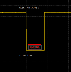
I am using BQ76952 BMS IC for battery managment with STM32 host microcontroller. Currently i am facing a problem regarding ALERT pin. I configure ALERT pin so that when any fault occure then that pin should interrupt to host microcontroller. By default this ALERT pin is at logic 1(3.3v). When a COV/CUV fault occure then CHG/DSG FET state is change but ALERT pin state is not changing. ALERT pin state should be change. I am checking the state of ALERT pin with CRO. Please suggest me what i am doing wrong while ALERT pin configuration.I am sharing below code..
/* USER CODE BEGIN Header */
/**
******************************************************************************
* @file : main.c
* @brief : Main program body
******************************************************************************
* @attention
*
* Copyright (c) 2023 STMicroelectronics.
* All rights reserved.
*
* This software is licensed under terms that can be found in the LICENSE file
* in the root directory of this software component.
* If no LICENSE file comes with this software, it is provided AS-IS.
*
******************************************************************************
*/
// BQ76952EVM demo code for STM32 NUCLEO-F103RB + BQ76952EVM
//
// Connection description: The I2C SCL and SDA pins are the only pin connections required between the
// NUCLEO board and the BQ76952EVM for this demo code. Also a ground connection should be made between the 2 boards.
// The ALERT, RST_SHUT, and DFETOFF pins are also configured on the MCU and can be used as shown.
//
// /|\ /|\
// STM32 5k |
// ----------------- | 5k
// | PB8 |---+---|-- I2C Clock (SCL)
// | | |
// | PB9 |-------+-- I2C Data (SDA)
// | |
// DFETOFF ---| PA8 |
// | |
// RST_SHUT ---| PA9 |--- Green LED
// | |
// ALERT ---| PA10 |
// | |
/* USER CODE END Header */
/* Includes ------------------------------------------------------------------*/
#include "main.h"
/* Private includes ----------------------------------------------------------*/
/* USER CODE BEGIN Includes */
#include <stdio.h>
#include "BQ769x2Header.h"
/* USER CODE END Includes */
/* Private typedef -----------------------------------------------------------*/
/* USER CODE BEGIN PTD */
/* USER CODE END PTD */
/* Private define ------------------------------------------------------------*/
/* USER CODE BEGIN PD */
#define DEV_ADDR 0x10 // BQ769x2 address is 0x10 including R/W bit or 0x8 as 7-bit address
#define CRC_Mode 0 // 0 for disabled, 1 for enabled
#define MAX_BUFFER_SIZE 10
#define R 0 // Read; Used in DirectCommands and Subcommands functions
#define W 1 // Write; Used in DirectCommands and Subcommands functions
#define W2 2 // Write data with two bytes; Used in Subcommands function
/* USER CODE END PD */
/* Private macro -------------------------------------------------------------*/
/* USER CODE BEGIN PM */
/* USER CODE END PM */
/* Private variables ---------------------------------------------------------*/
I2C_HandleTypeDef hi2c2;
TIM_HandleTypeDef htim1;
/* USER CODE BEGIN PV */
uint8_t RX_data [2] = {0x00, 0x00}; // used in several functions to store data read from BQ769x2
uint8_t RX_32Byte [32] = {0x00, 0x00, 0x00, 0x00, 0x00, 0x00, 0x00, 0x00, 0x00, 0x00, 0x00, 0x00, 0x00, 0x00, 0x00, 0x00,
0x00, 0x00, 0x00, 0x00, 0x00, 0x00, 0x00, 0x00, 0x00, 0x00, 0x00, 0x00, 0x00, 0x00, 0x00, 0x00};
//used in Subcommands read function
// Global Variables for cell voltages, temperatures, Stack voltage, PACK Pin voltage, LD Pin voltage, CC2 current
uint16_t CellVoltage [16] = {0x00,0x00,0x00,0x00,0x00,0x00,0x00,0x00,0x00,0x00,0x00,0x00,0x00,0x00,0x00,0x00};
float Temperature [3] = {0,0,0};
uint16_t Stack_Voltage = 0x00;
uint16_t Pack_Voltage = 0x00;
uint16_t LD_Voltage = 0x00;
uint16_t Pack_Current = 0x00;
uint16_t AlarmBits = 0x00;
uint8_t value_SafetyStatusA; // Safety Status Register A
uint8_t value_SafetyStatusB; // Safety Status Register B
uint8_t value_SafetyStatusC; // Safety Status Register C
uint8_t value_PFStatusA; // Permanent Fail Status Register A
uint8_t value_PFStatusB; // Permanent Fail Status Register B
uint8_t value_PFStatusC; // Permanent Fail Status Register C
uint8_t FET_Status; // FET Status register contents - Shows states of FETs
uint16_t CB_ActiveCells; // Cell Balancing Active Cells
uint8_t UV_Fault = 0; // under-voltage fault state
uint8_t OV_Fault = 0; // over-voltage fault state
uint8_t SCD_Fault = 0; // short-circuit fault state
uint8_t OCD_Fault = 0; // over-current fault state
uint8_t ProtectionsTriggered = 0; // Set to 1 if any protection triggers
uint8_t LD_ON = 0; // Load Detect status bit
uint8_t DSG = 0; // discharge FET state
uint8_t CHG = 0; // charge FET state
uint8_t PCHG = 0; // pre-charge FET state
uint8_t PDSG = 0; // pre-discharge FET state
uint32_t AccumulatedCharge_Int; // in BQ769x2_READPASSQ func
uint32_t AccumulatedCharge_Frac;// in BQ769x2_READPASSQ func
uint32_t AccumulatedCharge_Time;// in BQ769x2_READPASSQ func
/* USER CODE END PV */
/* Private function prototypes -----------------------------------------------*/
void SystemClock_Config(void);
static void MX_GPIO_Init(void);
static void MX_I2C2_Init(void);
static void MX_TIM1_Init(void);
/* USER CODE BEGIN PFP */
void delayUS(uint32_t us) { // Sets the delay in microseconds.
__HAL_TIM_SET_COUNTER(&htim1,0); // set the counter value a 0
while (__HAL_TIM_GET_COUNTER(&htim1) < us); // wait for the counter to reach the us input in the parameter
}
void CopyArray(uint8_t *source, uint8_t *dest, uint8_t count)
{
uint8_t copyIndex = 0;
for (copyIndex = 0; copyIndex < count; copyIndex++)
{
dest[copyIndex] = source[copyIndex];
}
}
unsigned char Checksum(unsigned char *ptr, unsigned char len)
// Calculates the checksum when writing to a RAM register. The checksum is the inverse of the sum of the bytes.
{
unsigned char i;
unsigned char checksum = 0;
for(i=0; i<len; i++)
checksum += ptr[i];
checksum = 0xff & ~checksum;
return(checksum);
}
unsigned char CRC8(unsigned char *ptr, unsigned char len)
//Calculates CRC8 for passed bytes. Used in i2c read and write functions
{
unsigned char i;
unsigned char crc=0;
while(len--!=0)
{
for(i=0x80; i!=0; i/=2)
{
if((crc & 0x80) != 0)
{
crc *= 2;
crc ^= 0x107;
}
else
crc *= 2;
if((*ptr & i)!=0)
crc ^= 0x107;
}
ptr++;
}
return(crc);
}
void I2C_WriteReg(uint8_t reg_addr, uint8_t *reg_data, uint8_t count)
{
uint8_t TX_Buffer [MAX_BUFFER_SIZE] = {0x00,0x00,0x00,0x00,0x00,0x00,0x00,0x00,0x00,0x00};
#if CRC_Mode
{
uint8_t crc_count = 0;
crc_count = count * 2;
uint8_t crc1stByteBuffer [3] = {0x10, reg_addr, reg_data[0]};
unsigned int j;
unsigned int i;
uint8_t temp_crc_buffer [3];
TX_Buffer[0] = reg_data[0];
TX_Buffer[1] = CRC8(crc1stByteBuffer,3);
j = 2;
for(i=1; i<count; i++)
{
TX_Buffer[j] = reg_data[i];
j = j + 1;
temp_crc_buffer[0] = reg_data[i];
TX_Buffer[j] = CRC8(temp_crc_buffer,1);
j = j + 1;
}
HAL_I2C_Mem_Write(&hi2c2, DEV_ADDR, reg_addr, 1, TX_Buffer, crc_count, 1000);
}
#else
HAL_I2C_Mem_Write(&hi2c2, DEV_ADDR, reg_addr, 1, reg_data, count, 1000);
#endif
}
int I2C_ReadReg(uint8_t reg_addr, uint8_t *reg_data, uint8_t count)
{
unsigned int RX_CRC_Fail = 0; // reset to 0. If in CRC Mode and CRC fails, this will be incremented.
uint8_t RX_Buffer [MAX_BUFFER_SIZE] = {0x00,0x00,0x00,0x00,0x00,0x00,0x00,0x00,0x00,0x00};
#if CRC_Mode
{
uint8_t crc_count = 0;
uint8_t ReceiveBuffer [10] = {0x00,0x00,0x00,0x00,0x00,0x00,0x00,0x00,0x00,0x00};
crc_count = count * 2;
unsigned int j;
unsigned int i;
unsigned char CRCc = 0;
uint8_t temp_crc_buffer [3];
HAL_I2C_Mem_Read(&hi2c2, DEV_ADDR, reg_addr, 1, ReceiveBuffer, crc_count, 1000);
uint8_t crc1stByteBuffer [4] = {0x10, reg_addr, 0x11, ReceiveBuffer[0]};
CRCc = CRC8(crc1stByteBuffer,4);
if (CRCc != ReceiveBuffer[1])
{
RX_CRC_Fail += 1;
}
RX_Buffer[0] = ReceiveBuffer[0];
j = 2;
for (i=1; i<count; i++)
{
RX_Buffer[i] = ReceiveBuffer[j];
temp_crc_buffer[0] = ReceiveBuffer[j];
j = j + 1;
CRCc = CRC8(temp_crc_buffer,1);
if (CRCc != ReceiveBuffer[j])
RX_CRC_Fail += 1;
j = j + 1;
}
CopyArray(RX_Buffer, reg_data, crc_count);
}
#else
HAL_I2C_Mem_Read(&hi2c2, DEV_ADDR, reg_addr, 1, reg_data, count, 1000);
#endif
return 0;
}
void BQ769x2_SetRegister(uint16_t reg_addr, uint32_t reg_data, uint8_t datalen)
{
uint8_t TX_Buffer[2] = {0x00, 0x00};
uint8_t TX_RegData[6] = {0x00, 0x00, 0x00, 0x00, 0x00, 0x00};
//TX_RegData in little endian format
TX_RegData[0] = reg_addr & 0xff;
TX_RegData[1] = (reg_addr >> 8) & 0xff;
TX_RegData[2] = reg_data & 0xff; //1st byte of data
switch(datalen)
{
case 1: //1 byte datalength
I2C_WriteReg(0x3E, TX_RegData, 3);
delayUS(2000);
TX_Buffer[0] = Checksum(TX_RegData, 3);
TX_Buffer[1] = 0x05; //combined length of register address and data
I2C_WriteReg(0x60, TX_Buffer, 2); // Write the checksum and length
delayUS(2000);
break;
case 2: //2 byte datalength
TX_RegData[3] = (reg_data >> 8) & 0xff;
I2C_WriteReg(0x3E, TX_RegData, 4);
delayUS(2000);
TX_Buffer[0] = Checksum(TX_RegData, 4);
TX_Buffer[1] = 0x06; //combined length of register address and data
I2C_WriteReg(0x60, TX_Buffer, 2); // Write the checksum and length
delayUS(2000);
break;
case 4: //4 byte datalength, Only used for CCGain and Capacity Gain
TX_RegData[3] = (reg_data >> 8) & 0xff;
TX_RegData[4] = (reg_data >> 16) & 0xff;
TX_RegData[5] = (reg_data >> 24) & 0xff;
I2C_WriteReg(0x3E, TX_RegData, 6);
delayUS(2000);
TX_Buffer[0] = Checksum(TX_RegData, 6);
TX_Buffer[1] = 0x08; //combined length of register address and data
I2C_WriteReg(0x60, TX_Buffer, 2); // Write the checksum and length
delayUS(2000);
break;
}
}
void CommandSubcommands(uint16_t command) //For Command only Subcommands
// See the TRM or the BQ76952 header file for a full list of Command-only subcommands
{ //For DEEPSLEEP/SHUTDOWN subcommand you will need to call this function twice consecutively
uint8_t TX_Reg[2] = {0x00, 0x00};
//TX_Reg in little endian format
TX_Reg[0] = command & 0xff;
TX_Reg[1] = (command >> 8) & 0xff;
I2C_WriteReg(0x3E,TX_Reg,2);
delayUS(2000);
}
void Subcommands(uint16_t command, uint16_t data, uint8_t type)
// See the TRM or the BQ76952 header file for a full list of Subcommands
{
//security keys and Manu_data writes dont work with this function (reading these commands works)
//max readback size is 32 bytes i.e. DASTATUS, CUV/COV snapshot
uint8_t TX_Reg[4] = {0x00, 0x00, 0x00, 0x00};
uint8_t TX_Buffer[2] = {0x00, 0x00};
//TX_Reg in little endian format
TX_Reg[0] = command & 0xff;
TX_Reg[1] = (command >> 8) & 0xff;
if (type == R) {//read
I2C_WriteReg(0x3E,TX_Reg,2);
delayUS(2000);
I2C_ReadReg(0x40, RX_32Byte, 32); //RX_32Byte is a global variable
}
else if (type == W) {
//FET_Control, REG12_Control
TX_Reg[2] = data & 0xff;
I2C_WriteReg(0x3E,TX_Reg,3);
delayUS(1000);
TX_Buffer[0] = Checksum(TX_Reg, 3);
TX_Buffer[1] = 0x05; //combined length of registers address and data
I2C_WriteReg(0x60, TX_Buffer, 2);
delayUS(1000);
}
else if (type == W2){ //write data with 2 bytes
//CB_Active_Cells, CB_SET_LVL
TX_Reg[2] = data & 0xff;
TX_Reg[3] = (data >> 8) & 0xff;
I2C_WriteReg(0x3E,TX_Reg,4);
delayUS(1000);
TX_Buffer[0] = Checksum(TX_Reg, 4);
TX_Buffer[1] = 0x06; //combined length of registers address and data
I2C_WriteReg(0x60, TX_Buffer, 2);
delayUS(1000);
}
}
void DirectCommands(uint8_t command, uint16_t data, uint8_t type)
// See the TRM or the BQ76952 header file for a full list of Direct Commands
{ //type: R = read, W = write
uint8_t TX_data[2] = {0x00, 0x00};
//little endian format
TX_data[0] = data & 0xff;
TX_data[1] = (data >> 8) & 0xff;
if (type == R) {//Read
I2C_ReadReg(command, RX_data, 2); //RX_data is a global variable
delayUS(2000);
}
if (type == W) {//write
//Control_status, alarm_status, alarm_enable all 2 bytes long
I2C_WriteReg(command,TX_data,2);
delayUS(2000);
}
}
void BQ769x2_Init() {
// Configures all parameters in device RAM
// Enter CONFIGUPDATE mode (Subcommand 0x0090) - It is required to be in CONFIG_UPDATE mode to program the device RAM settings
// See TRM for full description of CONFIG_UPDATE mode
CommandSubcommands(SET_CFGUPDATE);
// After entering CONFIG_UPDATE mode, RAM registers can be programmed. When programming RAM, checksum and length must also be
// programmed for the change to take effect. All of the RAM registers are described in detail in the BQ769x2 TRM.
// An easier way to find the descriptions is in the BQStudio Data Memory screen. When you move the mouse over the register name,
// a full description of the register and the bits will pop up on the screen.
// 'Power Config' - 0x9234 = 0x2D80
// Setting the DSLP_LDO bit allows the LDOs to remain active when the device goes into Deep Sleep mode
// Set wake speed bits to 00 for best performance
BQ769x2_SetRegister(PowerConfig, 0x2D80, 2);
// 'REG0 Config' - set REG0_EN bit to enable pre-regulator
BQ769x2_SetRegister(REG0Config, 0x01, 1);
// 'REG12 Config' - Enable REG1 with 3.3V output (0x0D for 3.3V, 0x0F for 5V)
BQ769x2_SetRegister(REG12Config, 0x0D, 1);
// Set DFETOFF pin to control BOTH CHG and DSG FET - 0x92FB = 0x42 (set to 0x00 to disable)
BQ769x2_SetRegister(DFETOFFPinConfig, 0x42, 1);
// Set up ALERT Pin - 0x92FC = 0x2A
// This configures the ALERT pin to drive high (REG1 voltage) when enabled.
// The ALERT pin can be used as an interrupt to the MCU when a protection has triggered or new measurements are available
BQ769x2_SetRegister(ALERTPinConfig, 0x2A, 1);
// Set TS1 to measure Cell Temperature - 0x92FD = 0x07
BQ769x2_SetRegister(TS1Config, 0x07, 1);
// Set TS3 to measure FET Temperature - 0x92FF = 0x0F
BQ769x2_SetRegister(TS3Config, 0x0F, 1);
// Set HDQ to measure Cell Temperature - 0x9300 = 0x07
BQ769x2_SetRegister(HDQPinConfig, 0x00, 1); // No thermistor installed on EVM HDQ pin, so set to 0x00
// 'VCell Mode' - Enable 16 cells - 0x9304 = 0x0000; Writing 0x0000 sets the default of 16 cells
BQ769x2_SetRegister(VCellMode, 0x0000, 2);
// Enable protections in 'Enabled Protections A' 0x9261 = 0xBC
// Enables SCD (short-circuit), OCD1 (over-current in discharge), OCC (over-current in charge),
// COV (over-voltage), CUV (under-voltage)
BQ769x2_SetRegister(EnabledProtectionsA, 0xBC, 1);
// Enable all protections in 'Enabled Protections B' 0x9262 = 0xF7
// Enables OTF (over-temperature FET), OTINT (internal over-temperature), OTD (over-temperature in discharge),
// OTC (over-temperature in charge), UTINT (internal under-temperature), UTD (under-temperature in discharge), UTC (under-temperature in charge)
BQ769x2_SetRegister(EnabledProtectionsB, 0xF7, 1);
// 'Default Alarm Mask' - 0x..82 Enables the FullScan and ADScan bits, default value = 0xF800
BQ769x2_SetRegister(DefaultAlarmMask, 0xF882, 2);
// Set up Cell Balancing Configuration - 0x9335 = 0x03 - Automated balancing while in Relax or Charge modes
// Also see "Cell Balancing with BQ769x2 Battery Monitors" document on ti.com
BQ769x2_SetRegister(BalancingConfiguration, 0x03, 1);
// Set up CUV (under-voltage) Threshold - 0x9275 = 0x31 (2479 mV)
// CUV Threshold is this value multiplied by 50.6mV
BQ769x2_SetRegister(CUVThreshold, 0x31, 1);
// Set up COV (over-voltage) Threshold - 0x9278 = 0x55 (4301 mV)
// COV Threshold is this value multiplied by 50.6mV
BQ769x2_SetRegister(COVThreshold, 0x55, 1);
// Set up OCC (over-current in charge) Threshold - 0x9280 = 0x05 (10 mV = 10A across 1mOhm sense resistor) Units in 2mV
BQ769x2_SetRegister(OCCThreshold, 0x05, 1);
// Set up OCD1 Threshold - 0x9282 = 0x0A (20 mV = 20A across 1mOhm sense resistor) units of 2mV
BQ769x2_SetRegister(OCD1Threshold, 0x0A, 1);
// Set up SCD Threshold - 0x9286 = 0x05 (100 mV = 100A across 1mOhm sense resistor) 0x05=100mV
BQ769x2_SetRegister(SCDThreshold, 0x05, 1);
// Set up SCD Delay - 0x9287 = 0x03 (30 us) Enabled with a delay of (value - 1) * 15 µs; min value of 1
BQ769x2_SetRegister(SCDDelay, 0x03, 1);
// Set up SCDL Latch Limit to 1 to set SCD recovery only with load removal 0x9295 = 0x01
// If this is not set, then SCD will recover based on time (SCD Recovery Time parameter).
BQ769x2_SetRegister(SCDLLatchLimit, 0x01, 1);
// Exit CONFIGUPDATE mode - Subcommand 0x0092
CommandSubcommands(EXIT_CFGUPDATE);
}
// ********************************* FET Control Commands ***************************************
void BQ769x2_BOTHOFF () {
// Disables all FETs using the DFETOFF (BOTHOFF) pin
// The DFETOFF pin on the BQ76952EVM should be connected to the MCU board to use this function
HAL_GPIO_WritePin(GPIOA, GPIO_PIN_8, GPIO_PIN_SET); // DFETOFF pin (BOTHOFF) set high
}
void BQ769x2_RESET_BOTHOFF () {
// Resets DFETOFF (BOTHOFF) pin
// The DFETOFF pin on the BQ76952EVM should be connected to the MCU board to use this function
HAL_GPIO_WritePin(GPIOA, GPIO_PIN_8, GPIO_PIN_RESET); // DFETOFF pin (BOTHOFF) set low
}
void BQ769x2_ReadFETStatus() {
// Read FET Status to see which FETs are enabled
DirectCommands(FETStatus, 0x00, R);
FET_Status = (RX_data[1]*256 + RX_data[0]);
DSG = ((0x4 & RX_data[0])>>2);// discharge FET state
CHG = (0x1 & RX_data[0]);// charge FET state
PCHG = ((0x2 & RX_data[0])>>1);// pre-charge FET state
PDSG = ((0x8 & RX_data[0])>>3);// pre-discharge FET state
}
// ********************************* End of FET Control Commands *********************************
// ********************************* BQ769x2 Power Commands *****************************************
void BQ769x2_ShutdownPin() {
// Puts the device into SHUTDOWN mode using the RST_SHUT pin
// The RST_SHUT pin on the BQ76952EVM should be connected to the MCU board to use this function
HAL_GPIO_WritePin(GPIOA, GPIO_PIN_9, GPIO_PIN_SET); // Sets RST_SHUT pin
}
void BQ769x2_ReleaseShutdownPin() {
// Releases the RST_SHUT pin
// The RST_SHUT pin on the BQ76952EVM should be connected to the MCU board to use this function
HAL_GPIO_WritePin(GPIOA, GPIO_PIN_9, GPIO_PIN_RESET); // Resets RST_SHUT pin
}
// ********************************* End of BQ769x2 Power Commands *****************************************
// ********************************* BQ769x2 Status and Fault Commands *****************************************
uint16_t BQ769x2_ReadAlarmStatus() {
// Read this register to find out why the ALERT pin was asserted
DirectCommands(AlarmStatus, 0x00, R);
return (RX_data[1]*256 + RX_data[0]);
}
void BQ769x2_ReadSafetyStatus() { //good example functions
// Read Safety Status A/B/C and find which bits are set
// This shows which primary protections have been triggered
DirectCommands(SafetyStatusA, 0x00, R);
value_SafetyStatusA = (RX_data[1]*256 + RX_data[0]);
//Example Fault Flags
UV_Fault = ((0x4 & RX_data[0])>>2);
OV_Fault = ((0x8 & RX_data[0])>>3);
SCD_Fault = ((0x8 & RX_data[1])>>3);
OCD_Fault = ((0x2 & RX_data[1])>>1);
DirectCommands(SafetyStatusB, 0x00, R);
value_SafetyStatusB = (RX_data[1]*256 + RX_data[0]);
DirectCommands(SafetyStatusC, 0x00, R);
value_SafetyStatusC = (RX_data[1]*256 + RX_data[0]);
if ((value_SafetyStatusA + value_SafetyStatusB + value_SafetyStatusC) > 1) {
ProtectionsTriggered = 1; }
else {
ProtectionsTriggered = 0; }
}
void BQ769x2_ReadPFStatus() {
// Read Permanent Fail Status A/B/C and find which bits are set
// This shows which permanent failures have been triggered
DirectCommands(PFStatusA, 0x00, R);
value_PFStatusA = (RX_data[1]*256 + RX_data[0]);
DirectCommands(PFStatusB, 0x00, R);
value_PFStatusB = (RX_data[1]*256 + RX_data[0]);
DirectCommands(PFStatusC, 0x00, R);
value_PFStatusC = (RX_data[1]*256 + RX_data[0]);
}
// ********************************* End of BQ769x2 Status and Fault Commands *****************************************
// ********************************* BQ769x2 Measurement Commands *****************************************
uint16_t BQ769x2_ReadVoltage(uint8_t command)
// This function can be used to read a specific cell voltage or stack / pack / LD voltage
{
//RX_data is global var
DirectCommands(command, 0x00, R);
if(command >= Cell1Voltage && command <= Cell16Voltage) {//Cells 1 through 16 (0x14 to 0x32)
return (RX_data[1]*256 + RX_data[0]); //voltage is reported in mV
}
else {//stack, Pack, LD
return 10 * (RX_data[1]*256 + RX_data[0]); //voltage is reported in 0.01V units
}
}
void BQ769x2_ReadAllVoltages()
// Reads all cell voltages, Stack voltage, PACK pin voltage, and LD pin voltage
{
int cellvoltageholder = Cell1Voltage; //Cell1Voltage is 0x14
for (int x = 0; x < 16; x++){//Reads all cell voltages
CellVoltage[x] = BQ769x2_ReadVoltage(cellvoltageholder);
cellvoltageholder = cellvoltageholder + 2;
}
Stack_Voltage = BQ769x2_ReadVoltage(StackVoltage);
Pack_Voltage = BQ769x2_ReadVoltage(PACKPinVoltage);
LD_Voltage = BQ769x2_ReadVoltage(LDPinVoltage);
}
uint16_t BQ769x2_ReadCurrent()
// Reads PACK current
{
DirectCommands(CC2Current, 0x00, R);
return (RX_data[1]*256 + RX_data[0]); // current is reported in mA
}
float BQ769x2_ReadTemperature(uint8_t command)
{
DirectCommands(command, 0x00, R);
//RX_data is a global var
return (0.1 * (float)(RX_data[1]*256 + RX_data[0])) - 273.15; // converts from 0.1K to Celcius
}
void BQ769x2_ReadPassQ(){ // Read Accumulated Charge and Time from DASTATUS6
Subcommands(DASTATUS6, 0x00, R);
AccumulatedCharge_Int = ((RX_32Byte[3]<<24) + (RX_32Byte[2]<<16) + (RX_32Byte[1]<<8) + RX_32Byte[0]); //Bytes 0-3
AccumulatedCharge_Frac = ((RX_32Byte[7]<<24) + (RX_32Byte[6]<<16) + (RX_32Byte[5]<<8) + RX_32Byte[4]); //Bytes 4-7
AccumulatedCharge_Time = ((RX_32Byte[11]<<24) + (RX_32Byte[10]<<16) + (RX_32Byte[9]<<8) + RX_32Byte[8]); //Bytes 8-11
}
// ********************************* End of BQ769x2 Measurement Commands *****************************************
/* USER CODE END PFP */
/* Private user code ---------------------------------------------------------*/
/* USER CODE BEGIN 0 */
/* USER CODE END 0 */
/**
* @brief The application entry point.
* @retval int
*/
int main(void)
{
/* USER CODE BEGIN 1 */
/* USER CODE END 1 */
/* MCU Configuration--------------------------------------------------------*/
/* Reset of all peripherals, Initializes the Flash interface and the Systick. */
HAL_Init();
/* USER CODE BEGIN Init */
/* USER CODE END Init */
/* Configure the system clock */
SystemClock_Config();
/* USER CODE BEGIN SysInit */
/* USER CODE END SysInit */
/* Initialize all configured peripherals */
MX_GPIO_Init();
MX_I2C2_Init();
MX_TIM1_Init();
/* USER CODE BEGIN 2 */
HAL_TIM_Base_Start(&htim1);
HAL_GPIO_WritePin(GPIOA, GPIO_PIN_9, GPIO_PIN_RESET); // RST_SHUT pin set low
HAL_GPIO_WritePin(GPIOA, GPIO_PIN_8, GPIO_PIN_RESET); // DFETOFF pin (BOTHOFF) set low
delayUS(10000);
CommandSubcommands(BQ769x2_RESET); // Resets the BQ769x2 registers
delayUS(60000);
BQ769x2_Init(); // Configure all of the BQ769x2 register settings
delayUS(10000);
CommandSubcommands(FET_ENABLE); // Enable the CHG and DSG FETs
delayUS(10000);
CommandSubcommands(SLEEP_DISABLE); // Sleep mode is enabled by default. For this example, Sleep is disabled to
// demonstrate full-speed measurements in Normal mode.
delayUS(60000); delayUS(60000); delayUS(60000); delayUS(60000); //wait to start measurements after FETs close
/* USER CODE END 2 */
/* Infinite loop */
/* USER CODE BEGIN WHILE */
while (1)
{
/* USER CODE END WHILE */
/* USER CODE BEGIN 3 */
///*
//Reads Cell, Stack, Pack, LD Voltages, Pack Current and TS1/TS3 Temperatures in a loop
//This basic example polls the Alarm Status register to see if protections have triggered or new measurements are ready
//The ALERT pin can also be used as an interrupt to the microcontroller for fastest response time instead of polling
//In this example the LED on the microcontroller board will be turned on to indicate a protection has triggered and will
//be turned off if the protection condition has cleared.
AlarmBits = BQ769x2_ReadAlarmStatus();
if (AlarmBits & 0x80) { // Check if FULLSCAN is complete. If set, new measurements are available
BQ769x2_ReadAllVoltages();
Pack_Current = BQ769x2_ReadCurrent();
Temperature[0] = BQ769x2_ReadTemperature(TS1Temperature);
Temperature[1] = BQ769x2_ReadTemperature(TS3Temperature);
DirectCommands(AlarmStatus, 0x0080, W); // Clear the FULLSCAN bit
}
if (AlarmBits & 0xC000) { // If Safety Status bits are showing in AlarmStatus register
BQ769x2_ReadSafetyStatus(); // Read the Safety Status registers to find which protections have triggered
if (ProtectionsTriggered & 1) {
HAL_GPIO_WritePin(GPIOC, GPIO_PIN_7, GPIO_PIN_SET); }// Turn on the LED to indicate Protection has triggered
DirectCommands(AlarmStatus, 0xF800, W); // Clear the Safety Status Alarm bits.
}
else
{
if (ProtectionsTriggered & 1) {
BQ769x2_ReadSafetyStatus();
if (!(ProtectionsTriggered & 1))
{
HAL_GPIO_WritePin(GPIOC, GPIO_PIN_7, GPIO_PIN_RESET);
}
} // Turn off the LED if Safety Status has cleared which means the protection condition is no longer present
}
delayUS(20000); // repeat loop every 20 ms
//*/
}
/* USER CODE END 3 */
}
/**
* @brief System Clock Configuration
* @retval None
*/
void SystemClock_Config(void)
{
RCC_OscInitTypeDef RCC_OscInitStruct = {0};
RCC_ClkInitTypeDef RCC_ClkInitStruct = {0};
/** Initializes the RCC Oscillators according to the specified parameters
* in the RCC_OscInitTypeDef structure.
*/
RCC_OscInitStruct.OscillatorType = RCC_OSCILLATORTYPE_HSI;
RCC_OscInitStruct.HSIState = RCC_HSI_ON;
RCC_OscInitStruct.HSICalibrationValue = RCC_HSICALIBRATION_DEFAULT;
RCC_OscInitStruct.Prediv1Source = RCC_PREDIV1_SOURCE_HSE;
RCC_OscInitStruct.PLL.PLLState = RCC_PLL_ON;
RCC_OscInitStruct.PLL.PLLSource = RCC_PLLSOURCE_HSI_DIV2;
RCC_OscInitStruct.PLL.PLLMUL = RCC_PLL_MUL9;
RCC_OscInitStruct.PLL2.PLL2State = RCC_PLL_NONE;
if (HAL_RCC_OscConfig(&RCC_OscInitStruct) != HAL_OK)
{
Error_Handler();
}
/** Initializes the CPU, AHB and APB buses clocks
*/
RCC_ClkInitStruct.ClockType = RCC_CLOCKTYPE_HCLK|RCC_CLOCKTYPE_SYSCLK
|RCC_CLOCKTYPE_PCLK1|RCC_CLOCKTYPE_PCLK2;
RCC_ClkInitStruct.SYSCLKSource = RCC_SYSCLKSOURCE_PLLCLK;
RCC_ClkInitStruct.AHBCLKDivider = RCC_SYSCLK_DIV1;
RCC_ClkInitStruct.APB1CLKDivider = RCC_HCLK_DIV1;
RCC_ClkInitStruct.APB2CLKDivider = RCC_HCLK_DIV1;
if (HAL_RCC_ClockConfig(&RCC_ClkInitStruct, FLASH_LATENCY_1) != HAL_OK)
{
Error_Handler();
}
/** Configure the Systick interrupt time
*/
__HAL_RCC_PLLI2S_ENABLE();
}
/**
* @brief I2C2 Initialization Function
* @param None
* @retval None
*/
static void MX_I2C2_Init(void)
{
/* USER CODE BEGIN I2C2_Init 0 */
/* USER CODE END I2C2_Init 0 */
/* USER CODE BEGIN I2C2_Init 1 */
/* USER CODE END I2C2_Init 1 */
hi2c2.Instance = I2C2;
hi2c2.Init.ClockSpeed = 400000;
hi2c2.Init.DutyCycle = I2C_DUTYCYCLE_2;
hi2c2.Init.OwnAddress1 = 0;
hi2c2.Init.AddressingMode = I2C_ADDRESSINGMODE_7BIT;
hi2c2.Init.DualAddressMode = I2C_DUALADDRESS_DISABLE;
hi2c2.Init.OwnAddress2 = 0;
hi2c2.Init.GeneralCallMode = I2C_GENERALCALL_DISABLE;
hi2c2.Init.NoStretchMode = I2C_NOSTRETCH_DISABLE;
if (HAL_I2C_Init(&hi2c2) != HAL_OK)
{
Error_Handler();
}
/* USER CODE BEGIN I2C2_Init 2 */
/* USER CODE END I2C2_Init 2 */
}
/**
* @brief TIM1 Initialization Function
* @param None
* @retval None
*/
static void MX_TIM1_Init(void)
{
/* USER CODE BEGIN TIM1_Init 0 */
/* USER CODE END TIM1_Init 0 */
TIM_ClockConfigTypeDef sClockSourceConfig = {0};
TIM_MasterConfigTypeDef sMasterConfig = {0};
/* USER CODE BEGIN TIM1_Init 1 */
/* USER CODE END TIM1_Init 1 */
htim1.Instance = TIM1;
htim1.Init.Prescaler = 36-1;
htim1.Init.CounterMode = TIM_COUNTERMODE_UP;
htim1.Init.Period = 65535;
htim1.Init.ClockDivision = TIM_CLOCKDIVISION_DIV1;
htim1.Init.RepetitionCounter = 0;
htim1.Init.AutoReloadPreload = TIM_AUTORELOAD_PRELOAD_DISABLE;
if (HAL_TIM_Base_Init(&htim1) != HAL_OK)
{
Error_Handler();
}
sClockSourceConfig.ClockSource = TIM_CLOCKSOURCE_INTERNAL;
if (HAL_TIM_ConfigClockSource(&htim1, &sClockSourceConfig) != HAL_OK)
{
Error_Handler();
}
sMasterConfig.MasterOutputTrigger = TIM_TRGO_RESET;
sMasterConfig.MasterSlaveMode = TIM_MASTERSLAVEMODE_DISABLE;
if (HAL_TIMEx_MasterConfigSynchronization(&htim1, &sMasterConfig) != HAL_OK)
{
Error_Handler();
}
/* USER CODE BEGIN TIM1_Init 2 */
/* USER CODE END TIM1_Init 2 */
}
/**
* @brief GPIO Initialization Function
* @param None
* @retval None
*/
static void MX_GPIO_Init(void)
{
GPIO_InitTypeDef GPIO_InitStruct = {0};
/* GPIO Ports Clock Enable */
__HAL_RCC_GPIOB_CLK_ENABLE();
__HAL_RCC_GPIOC_CLK_ENABLE();
__HAL_RCC_GPIOA_CLK_ENABLE();
/*Configure GPIO pin Output Level */
HAL_GPIO_WritePin(GPIOC, GPIO_PIN_7, GPIO_PIN_RESET);
/*Configure GPIO pin Output Level */
HAL_GPIO_WritePin(GPIOA, GPIO_PIN_8|GPIO_PIN_9, GPIO_PIN_RESET);
/*Configure GPIO pin : PC7 */
GPIO_InitStruct.Pin = GPIO_PIN_7;
GPIO_InitStruct.Mode = GPIO_MODE_OUTPUT_PP;
GPIO_InitStruct.Pull = GPIO_NOPULL;
GPIO_InitStruct.Speed = GPIO_SPEED_FREQ_LOW;
HAL_GPIO_Init(GPIOC, &GPIO_InitStruct);
/*Configure GPIO pins : PA8 PA9 */
GPIO_InitStruct.Pin = GPIO_PIN_8|GPIO_PIN_9;
GPIO_InitStruct.Mode = GPIO_MODE_OUTPUT_PP;
GPIO_InitStruct.Pull = GPIO_NOPULL;
GPIO_InitStruct.Speed = GPIO_SPEED_FREQ_LOW;
HAL_GPIO_Init(GPIOA, &GPIO_InitStruct);
}
/* USER CODE BEGIN 4 */
/* USER CODE END 4 */
/**
* @brief This function is executed in case of error occurrence.
* @retval None
*/
void Error_Handler(void)
{
/* USER CODE BEGIN Error_Handler_Debug */
/* User can add his own implementation to report the HAL error return state */
__disable_irq();
while (1)
{
}
/* USER CODE END Error_Handler_Debug */
}
#ifdef USE_FULL_ASSERT
/**
* @brief Reports the name of the source file and the source line number
* where the assert_param error has occurred.
* @param file: pointer to the source file name
* @param line: assert_param error line source number
* @retval None
*/
void assert_failed(uint8_t *file, uint32_t line)
{
/* USER CODE BEGIN 6 */
/* User can add his own implementation to report the file name and line number,
ex: printf("Wrong parameters value: file %s on line %d\r\n", file, line) */
/* USER CODE END 6 */
}
#endif /* USE_FULL_ASSERT */
Thanks with regards
Deepak