This thread has been locked.

If you have a related question, please click the "Ask a related question" button in the top right corner. The newly created question will be automatically linked to this question.

TPS1H000-Q1: Why PIN 7 and PIN8 burned down during PIN7 short to GND

Part Number: TPS1H000-Q1
Other Parts Discussed in Thread: TPS1H000EVM

TEST SETUP.pdf

Hello,

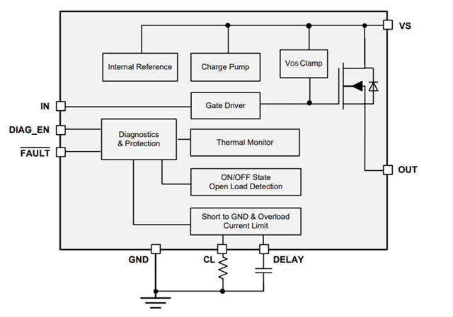
In our application, TPS1H000-Q1 is used for High side swith, detail block diagram in attached page 1. PIN7 is PWM output and will be connect to vehicle side other ECU.

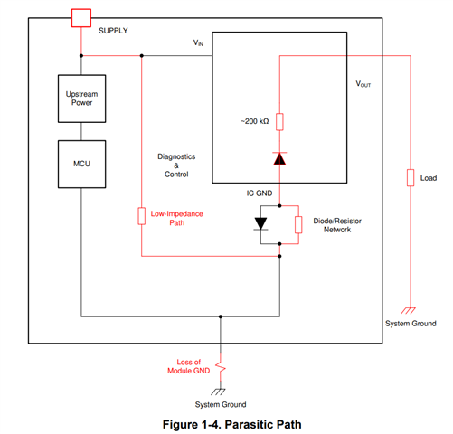
There is a customer test requirement, the setup show in page 2: The board connect to battery but GND is fload, and the IC PIN7 need to connect to GND. In this test case, we found IC(TPS1H000-Q1) PIN8 and PIN7 burned down.

In order to find the reason, we did page3 and page 4 debug. In page3, cut all input between MCU and IC(TPS1H000-Q1), repeat the test. still found PIN8 and PIN7 burned down. In page4, cut all input between MCU and IC(TPS1H000-Q1) and remove the diode D1, repeat the test, no burned down between pin8 and pin7, meanwhile, both MCU and BUCK are work well, but there is a 2V between IC PIN6 and DC 12V "-" side.

May I know what will be happened during our page3 test? why PIN 7 and PIN8 burned down?

what is the internal connection between PIN7 and GND(PIN6)?

  • Jingjing,

    In the case you are describing, you have a loss-of-ground issue AND a short-to-ground on the output. These sort of issues are considered double fault issues and there is not a way for us to give a reliable mitigation plan when multiple catastrophic faults are happening in the system. We have not seen double faults as a particular requirement with common automotive customers- is there any specific functional safety requirement that this system is being designed to?

  • Hi, Timothy,

    Thanks to reply fristly!

    You are right that the test case is a loss-of-ground issue AND a short-to-ground on the output.

    Understood that you mentioned "there is not a way for us to give a reliable mitigation plan when multiple catastrophic faults are happening in the system". The test case is from customer requirement, and they mentention such case maybe happenned during their production line. 

     Now customer request us to give the deep analysis what will be happened during our page2 test? What is broken in side of IC? Now big pressure from customer...Could you share us more detail circuit of inside IC? Or any other suggestion to find the root cause?

    By the way, We also confuse why still work and with 2V between IC PIN6 and DC 12V "-" side in page 4. Would you please give us more explain too?

    Thanks in advance!

  • Jingjing,

    During a loss-of-ground issue the output of the device is shut off- regardless of the state of the EN pin. The only way that damage could occur in this case if there was significant reverse current going from the output, through the body diode of the FET, and to the supply. We do not explicitly rate the body diode of the FET so if this is the case you need to have something like a blocking diode on the input.

    We are not able to share a detailed diagram of the internal working of the device, but would be happy to clarify any points in the datasheet that you might have questions on. If you suspect a quality issue, please submit a request at https://ticsc.service-now.com/csm/?_ticdt=MTY4MDE4NDEzM3wwMTg3MmZiYTk5NDcwMDA0ZTI5MzcwODgyYjRkMDUwNmYwMDhhMDY3MDBmYjh8R0ExLjIuNjAyOTkxNTA1LjE2ODAxMzI5NzE.

    Could you share the schematic of the design? Furthermore, as we are not seeing this with our local testing in Dallas, I would request for you to run this test on the TPS1H000EVM. This will give you the best component set, ideal layout, etc. for testing your application.

  • tps1h000 circuit.pdf

    Hi, Timothy,

    Attached is our circuit in the application, I share buck circuit too for analysis. Please kindly help to give your suggestion.

    Unfortunately, there isn't EVM boad in our hands, we are working on apply from our local support, we will do further test after get it.

    We wonder the body diode broken cause by inush current of system, serial a resistor can solve this problem in our application. But customer insist on pushin g us to give the deep analysis what will be happened during our page2 test, and what is broken in side of IC.

  • Jingjing,

    We aren't able to provide any detailed level view of the internal device circuitry as this is considered proprietary, however the block diagram in the datasheet should give a good understanding of what is happening in the system:

    What I believe is happening here is with the double fault condition they are running into the parasitic path described in https://www.ti.com/lit/pdf/slvaes9 100

    It does sound like there could be some application variables in this system like other parasitic paths or soldering/setup issues. To make sure to eliminate all variables, please try to work with the local TI team to get an EVM so that you can test with a known good setup.

  • Hi, Timothy,

    Today, The root cause is found: System innrush current was too big during power on. After remove some caps on the board, without burned down. 

    One point confused us: In the file(test setup.pdf) page4, the inrush current also exist during power on. Why no burned down in the test? May I know any hint from you?

    Thanks in advance!

  • Jingjing,

    I am a little unclear from the diagram- but what I would suspect is happening is that there might be too much current going through the body diode of the FET. We do not rate the body diode of the FET so if there is too much power being dissipated across it this could potentially lead to damage. 

  • Hi, Timothy,

    Sorry you can not find capacitors in the attached since they are not suspicious of relevant at beginning. Those capacitors are on battery line in our system, they didn't show in the attached. 

    You are right too much inrush current going through the TPS1H000-Q1 GND PIN during test at beginning. It was measured during test. But we are not clear how to work inside IC to lead PIN 7 and PIN8 burned down.

    We already show related information to customer and explain to them that any detailed level view of the internal device circuitry can not be provided yesterday. They accept the status and topic closed unless further information comming currently. I will close this issue too. 

    Thanks.