This thread has been locked.

If you have a related question, please click the "Ask a related question" button in the top right corner. The newly created question will be automatically linked to this question.

LMQ61460: switching frequency fluctuates

Part Number: LMQ61460


Dear TI experts,

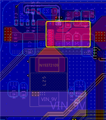
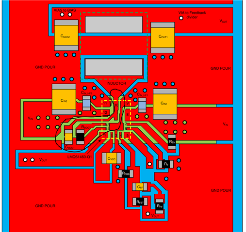
We are seeing a strange behavior of our LMQ61460 circuit. It is designed for 12V to 32V input, output 9.3V/5.5A, 450KHz switching frequency. Schematic is shown below.

So far it works and can deliver 5.5A output as expected. But we observed that the switching frequency keeps on jumping up and down from 180KHz to about 800KHz. Please see switched node waveform captured at 3A output current. The output voltage ripple waveform also shows strange frequency of 104KHz and peak-peak ripple of 280mV which is too high.

The Cff is not mounted initially. But we already tried 1Kohm and 22pF for Rff and Cff (on the place of C183 in schematic) and they did not help.

Is this indicating some instability issue? And what could be the cause? Could you please help?

Thank you.

  • Hi,

    The switch node should be a constant square wave. The image you have shown for SW look unstable. 

    I would suggest increasing the output capacitance from 55uF to 100uF and retest.

    WEBENCH designer tool for a VIN = 12V - 32V, VOUT = 9.3A, IOUT = 5.5A, FSW = ~450kHz suggests 2 x 47uF output capacitance. 

    https://webench.ti.com/appinfo/webench/scripts/SDP.cgi?ID=256AD355238E8343

    Regards,

    Jimmy

  • Hi Jimmy,

    Thanks for your prompt feedback.

    I have tried adding 47uF capacitor on the output but nothing changes. I also checked the bootstrap voltage and VCC voltage, they all look fine. Any idea what else I can try?

    Here are screenshots of the layout, if you want to have a look. We tried to follow the reference in datasheet as much as possible. It is 8-layer, and the circuit is on L8 (bottom).

    L8:

    L7 is fully grounded.

    L6: there is a copper shape of the switching node connection. This is not good, but I think it is already shielded by the GND on adjacent layers. Could it be the cause?

    Regards,

    Tuan.

  • Hi Tuan,

    How many of your boards are experiencing this issue? Again judging from your schematic it looks to be similar to what is recommended in the WEBENCH designer tool the schematic looks okay so I suspect it is a PCB layout issue. 

    As you've pointed out the large SW node that has vias to the inner layer of the boards which is not recommended. Also note that the datasheet suggest to route the SW connection under the device through the gap between VIN2 and RBOOT pins, reducing exposed SW node area. 

    The recommended PCB layout would have as small as possible to prevent noise coupling to the SW and only on the top layer. You would have to look not only at the SW cooper plane but also at the SW vias and if it is close to any noising signal traces on the inner layers. Because of this it its not recommended to have SW vias through the board. 

    See example of EVM layout below. 

    Regards,

    Jimmy

  • Hi Jimmy,

    We have tested on 3 boards and they show the same behavior.

    Thanks for the layout guideline, we will try to follow for the next sample build. But for this prototype do you have other suggestions which we can try out?

    Regards,

    Tuan.

  • Hi Tuan,

    I would suggest you take the LMQ61460EVM and swap the components on the EVM with  your own values to validate design operation.

    This way while you are waiting for the next sample builds to implement the revision, you can evaluate the part using TI recommended PCB layout.

    Regards,

    Jimmy