This thread has been locked.

If you have a related question, please click the "Ask a related question" button in the top right corner. The newly created question will be automatically linked to this question.

LMG1205: Ho,Lo output problem

Part Number: LMG1205
Other Parts Discussed in Thread: LMG1210

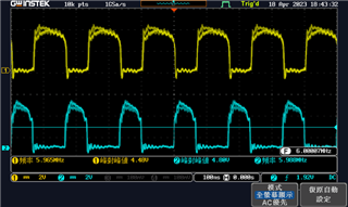
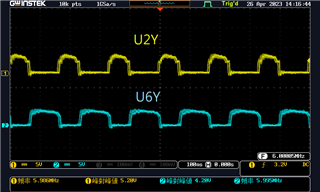
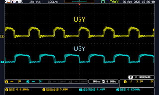
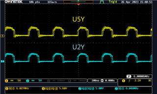
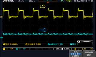
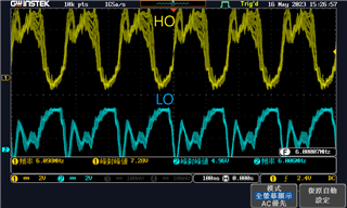
This is my HI and LI signals, but the Ho and Lo signals are not staggered.
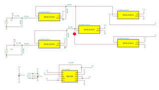
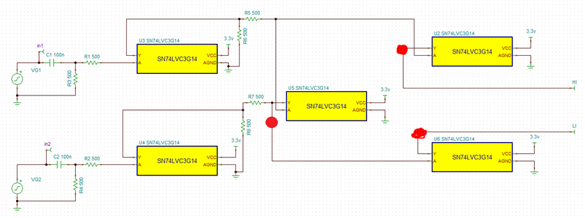
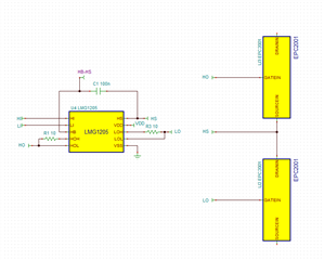
This is my circuit.

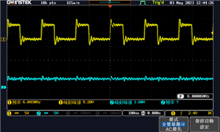
IN1 inputs a 6MHz square wave, and IN2 inputs a 500kHz sine wave. These two signals are modulated by an inverter to generate two opposite 6MHz PWM signals, HI and LI.


  • Hi Jia-Hua,

    Thank you for reaching out! It looks like your inputs are working and show different duty cycles, but the outputs share the same duty cycle and both appear to match one of the input waveforms. This could be caused by something shorting the inputs together. You could test this by grounding one of the inputs and seeing if you still get two output waveforms, or no output waveforms. Also, where are you measuring HI and LI? Are you measuring directly at the pins?

    Best,

    Alex Weaver

  • I have tested and found that the presence or absence of input on IN2 does not affect the output, only when there is input on IN1 will there be two outputs.

    I can only measure the signal of IN1 at the red dot location.

    I have measured the outputs of the inverter and the HI and LI of LMG1205, all directly at the pins.

  • Hi Jia-Hua,

    It sounds like you have confirmed that the input signals are converging before arriving to the gate driver. If only IN1 is effecting the output, it looks like something happened to your IN2 signal to short/converge with IN1. This could be due to the orientation of the inverters, or solder shorting the two paths together. Could you try measuring the continuity at the red dots in the schematic:

    Specifically, I am hoping you can measure the continuity of the Y pins of U2 and U6. This could help us narrow down where the signals converge.

    Best,

    Alex Weaver

  • This is the output of pins Y for U6 and U2, as well as the output of U5Y.

    I am planning to mix a 500 kHz sine wave, which has been converted to a square wave via an inverter, with a 6 MHz square wave using U5Y.

    To test the LMG1205, do I only need to input HI and LI and observe the HO and LO outputs? Currently, the GaN FET is not being powered.

  • Hi Jia-Hua,

    You are correct, you will only need HI, LI, LO, and HO for this debug. You will not want to power the FETs in the current state, as the output signals not being staggered would cause shoot through and damage the GaN FETs.

    It looks like the U2Y and U6Y signals are properly staggered and creating the correct input signals, so the issue is most likely with the soldering between HI and LI. As you can see from the LMG1205 pinout below, the LI and HI pins are located next to each other on the device:

    You might want to consider re-soldering the device, or investigating if there is a noticeable short in the board between the LI and HI traces.

    Best,

    Alex Weaver

  • When I tested it before, the FET was connected but there was no power supplied.

    After removing the circuit of the FET section, I found that only the LO part had a waveform, and the HO part did not have a clear waveform.

  • Hi Jia-Hua,

    Can you confirm which components you removed to disconnect the FET circuitry? Did you remove any gate resistors, the FETs, or any capacitors?

    Also, can you confirm where the outputs are being measured to generate those waveforms?

    Best,

    Alex Weaver

  • Only remove the FET.

    I left the HO, LO, and HS of LMG1205 unconnected and measured the waveforms of HO and LO. I am not sure if these waveforms are correct.

  • Hi Jia Hua,

    The HO output is normally measured as the differential voltage HO-HS, and I suspect the reason you are getting a non-zero value is because you are measuring HO with respect to ground. The HO output is not switching, so I believe the device may have been damaged by shoot-through (both outputs being on at the same time). Here is an image of the switching waveforms from the LMG1205 EVM User's Guide:

    The blue output is the LO signal, and the green output is HO. You could try using a single PWM input (HI) and grounding the LI input signal to confirm if the outputs are functioning. The device should be able to create a complimentary output signal based on the single input.

    Best,

    Alex Weaver

  • I have two outputs now after replacing a set of FETs.

    The output at a working frequency of 1 MHz.

    Is there any way to improve the output waveform at 6 MHz?

  • Hi Jia-Hua,

    I'm glad to hear you were able to get the driver functioning properly! I'm going to link an article for optimizing multi-megahertz operation of GaN drivers, specifically LMG1210. You could try implementing a Schottky diode or PN junction diode to help with reverse recovery losses. If you choose to implement a Schottky diode, you will want to focus on choosing a diode with low forward voltage drop and low junction capacitance.

    Also, is your system experiencing noise on the inputs? You might consider implementing an RC input filter to help remove noise from the system.

    Best,

    Alex Weaver