


Other Parts Discussed in Thread: LM25149-Q1
Hello,
I've designed a board with LM25148 to reach 5V out @ 8A with 15V in.
I've used the datasheet and WebEnch to create the design.
I'm testing the design with an electronic load. It's ok upto 3.0A with VOut = 5.02V .
At 3.1A, PGood goes low and VOut fall to 4.33V. VOut stays at 4.33V upto 5A. I can reach 11A with VOut=3V.
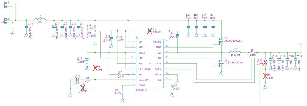
Schematic
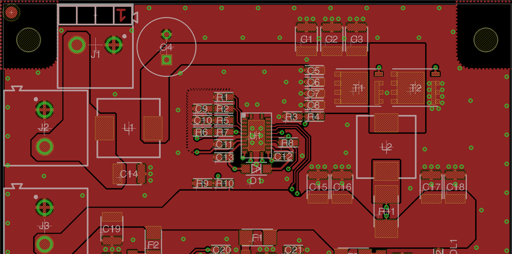
Top Layout
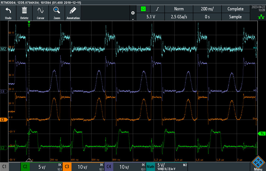
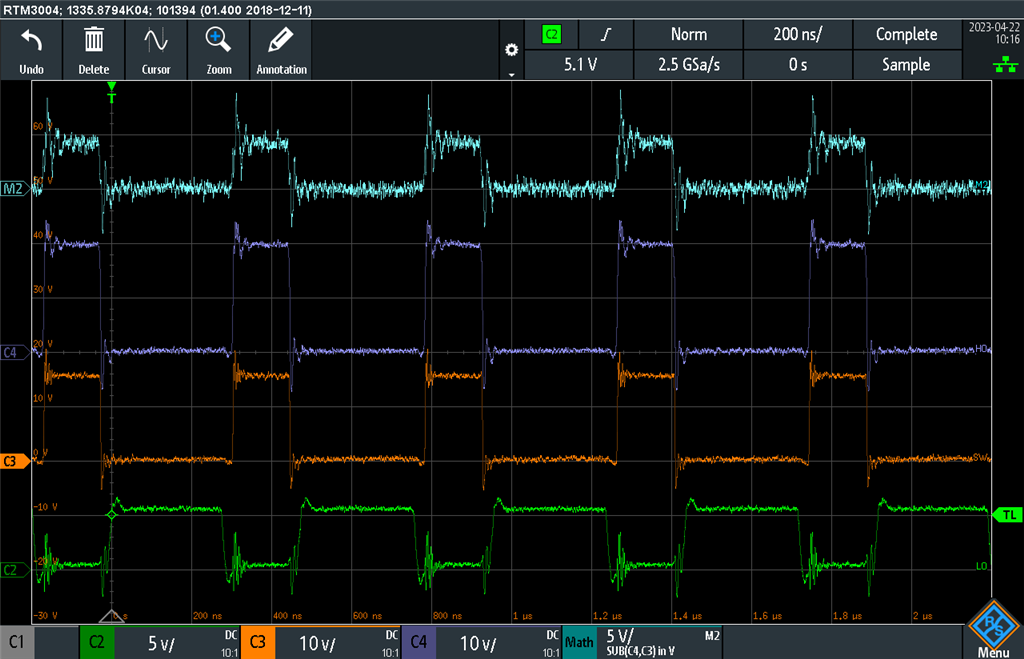
No Load: C2->LO ; C3-> SW; C4-> HO; Math -> HO Minus SW
2A Load. VOut = 5.02V
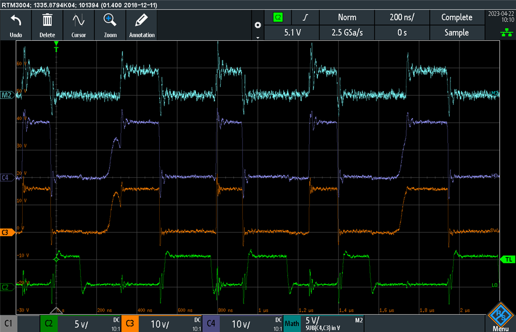
4A Load, VOut drops to 4.33V
Any idea or clue ?
Thank you for your help.
