This thread has been locked.

If you have a related question, please click the "Ask a related question" button in the top right corner. The newly created question will be automatically linked to this question.

TPS7A84: TPS7A84: FB have a overshoot and undershoot when VIN power off

Part Number: TPS7A84
Other Parts Discussed in Thread: TEST2

Hi team,

This is FAE Jayden, my customer use TPS7A8401, there is a fault that needs help to confirm:

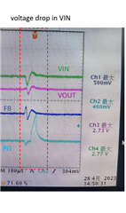
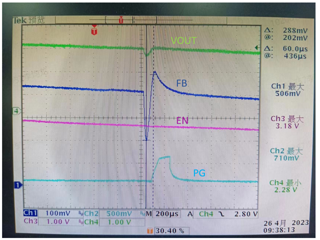
Application: 3.6Vin~3.3Vout, Vout adjusted by using external FB resistors; When Vin power off, there is voltage drop in Vout , likewise there is a voltage drop and overshoot in FB, and the PG signal also has voltage.

Therefore, I would like to ask what may be the root cause of the FB voltage overshoot and undershoot?

Brs

Jayden

  • Hi Jayden,

    It is not clear to me what is happening in this oscilloscope plot. You said VIN is powered off, but VIN is not included in the plot. Why is EN slowly drooping? It looks like all signals are slowly drooping. Was the device already on and then the input is removed? Is the fact that you want to change the output by switching resistors relevant to the issue you're trying to show? I need more information to look at this.

    Regards,

    Nick

  • TPS7A8401 FB issues.pptx

    Hi Nick,

    Thanks for your reply and sorry for late response. I have checked with ZTE and I have shown the BOM in the attached slides and described the problem specifically. Pls let me know if any issues. Thanks.

    Look forward to your reply.

    Brs 

    Jayden

  • Hi Jayden,

    It seems that the customer does not understand the basics of LDOs. When they bring VIN below VOUT, the device is in dropout and cannot regulate. Hence, any time VIN changes in this condition, VOUT follows. This appears to be happening in every test that they show. Furthermore, I calculate a set output voltage of 5.3V with the feedback resistors they have drawn, so the device is always in dropout anyways. 

    Regards,

    Nick

  • Hi Nick, 

    Thanks for reply. They use TPS7A8401A, so the Vref=0.5V and the target output voltage is 3.3V with the feedback resistors. But in this case it is indeed in the voltage dropout and cannot regulate. 

    I still have questions about test 3. When VIN has a voltage drop, why does FB increase first and then decrease? And when the FB voltage rises, the PG signal is not pulled high immediately, but there seems to be a delay? Many Thanks.

    BRs

    Jayden

  • Hi Jayden,

    I see. It looks to me like VOUT actually goes up a little before going back down as well so this seems consistent to me. I don't know why the FB voltage spikes higher than VOUT does, but I don't think this is worth much consideration because this is the device operating in dropout anyways. 

    As for the PG question, PG has a kind of propagation delay so it is not surprising that it is not immediate. 

    Regards,

    Nick

  • Hi Nick,

    Thanks. I think it may be the effect of Cff =10nF that causes the voltage of FB to be higher than the voltage of VOUT.

    It seems that PG doesn't have propagation delay in test1 and test2.

    Brs

    Jayden