This thread has been locked.

If you have a related question, please click the "Ask a related question" button in the top right corner. The newly created question will be automatically linked to this question.

TPS54302: Unable to get stable output and issues with IC shut-off

Part Number: TPS54302

Hi,

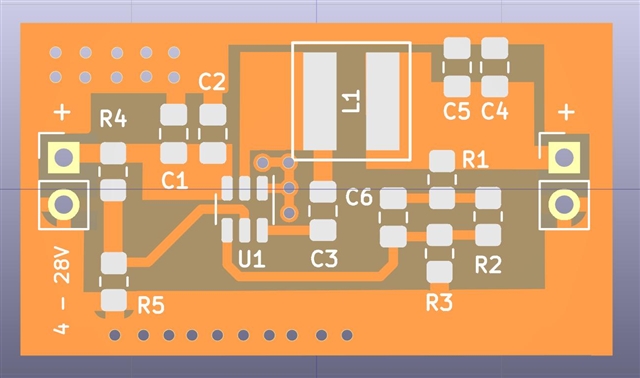
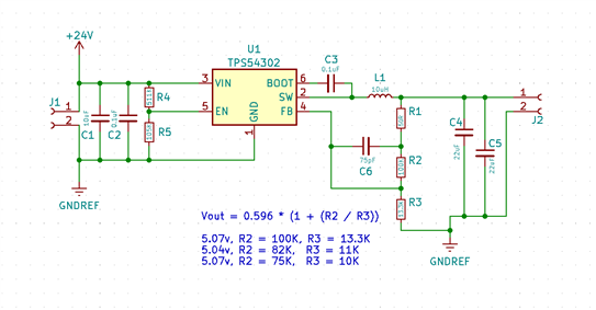
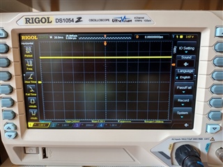
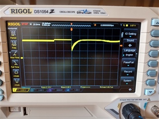
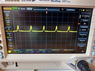
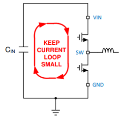
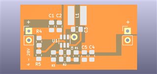
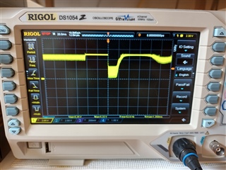
I'm trying to use TPS54302DDCR for a 24V to 5V / 500mA step down supply with the following layout and components. I seem to get output voltage glitches when at around 100mA load where the voltage drops 1-2V for 100us and beyond 250mA the IC goes into some sort of PWM / shut-off where I can see voltage pulsing between 500mV and ~2V. Is there something wrong with the layout ? Thanks

C1 = 10uF X7R

C2 = 0.1uF X7R

C3 =0.1uF X7R

C4 = 10uF X7R

C5 = 22uF X7R

C6 = 75pF X7R

R1 = 50R 1%

R2 = 75K 1%

R3 = 10K 1%

R4 = 510K 1%

R5 = 100K 1%

L1 = 10uH CDRH4D28NP-100NC

  • Hi ,

    I didn't see your sch , and could you help capture some wavefroms for analysis.

    The layout is not really good, you can refer this EVM layout .6597874D.zip

  • Hi,

    I'm not a design expert, so it would be very helpful if you could point out what's wrong with the layout I shared.

    I've kept the power traces as wide as possible, the entire bottom layer is a ground plane and the feedback / boost gap is as wide as I can make it.

    Schematic

    This is how it looks without load

    No Load

    Glitch with 250ma load

    Shutdown at 400ma

  • Hi

    1. Vin Trace(Pin3)

        1) Vin trace is not large enough

        2)Close loop is too large

    2. SW (Pin2)

      1) Pls keep the SW trace as physically short and wide as practical to minimize radiated emissions.

    3.GND(Pin3)

       1)GND traces should be as wide as possible to reduce trace impedance

    4.FB(Pin4)

       1)The trace of the FB should be as small as possible to avoid noise coupling

       2) FB node (R2,R3 connection point) should be as close to FB pin.

       3)Voltage feedback loop should be placed away from the high-voltage switching trace, and preferably has ground shield.

       4) Vout sense point should be close to Vout cap.

    5. EN (Pin5)

        1) EN trace is not that critical, no need large trace

  • Thanks heaps Young, that is very helpful. I'll make the suggested changes.

  • Hi Young,

    I made the recommended changes, but I've still kept the ground on pin one going through a large via with solid copper infill. The change has improved the response, I no longer see the converter going into a shutdown at high load (500mA) but I can still see the periodic glitch where the output voltage drops to 0V and goes back up again. I've played with inductor choices going up to CDRH74NP-100  (10uH, 1.84A, ~50mΩ DCR).

    Any idea where I should be looking to fix this ? Thanks

  • Hi,

    what happened during this  periodic glitch? 

    and if it's possible to get one EVM to replace the current layout/design on our board , to check if no issue with EVM ? or still can repeat ?

  • Hi Young,

    The test setup feeds in 24V 1A max (CV/CC) with an Agilent U8002A, constant current load at 250mA. When the glitch happens, I can see the input current spiking and dropping back. I've added an additional 330uF capacitor close to the input and an additional 330uF capacitor at output to smooth out at spikes.

    Do you notice anything obviously wrong in the layout ?  I can look at buying TPS54302EVM-716 from TI, local suppliers don't have stock.

    Thanks

  • Hi Harold,

    Young will check it then feedback you soon.

  • Hi ,

    Frankly this layout is still not good, suggest to get one EVM to check.

    And better capture Vin+SW+Vout+indcutor current together for analysis.

  • Hi Young,

    I think I fixed the issue, no big changes to the layout. I changed the inductor to CDRH104-100NC and added an extra 22uF input bypass and an extra 22uF output filter capacitor.

    I'm not sure what the original issue was, but no glitching in 2 test boards so far. I kept the design as is since it allows me to have a solid ground plane at the bottom and the output noise / ripple is low <100mv at 750mA load.

    Thanks