This thread has been locked.

If you have a related question, please click the "Ask a related question" button in the top right corner. The newly created question will be automatically linked to this question.

TLV62090: Unable to achieve low current regulation

Part Number: TLV62090

Hi,

I have three TLV62090's operating as current regulators. I adjust the current by tracking a voltage at the SS pin. The minimum current is set by R1 and R2 (R2 actually goes through a PWM driver, and so here duty=0).

The models both in Tina and in LTSpice both indicate the lowest current regulation of 30mA, which is the requirement.

In real-life the lowest current through the load is measured as 275mA by ADC with 256x oversampling, or 239mA by Bryen BM896 multimeter (about as good as it gets). Either way it's a long way off the required 30mA.

Any clues much appreciated!

Andrew


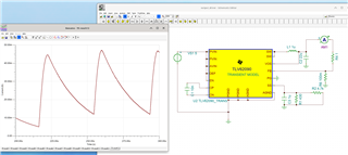
output_driver.tsc.zip

  • Hi Andrew,

    It's an unusual way to use the voltage regulator. But I guess what you are trying should probably work. 

    Since you are seeing a higher current through your load (the FB divider resistors), you could try to bring the VOUT even lower. Can you try reducing the SS voltage by reducing the values of R1 or R2? Or in case the PWM driver is used, then either the voltage or the duty of this signal.

    Could you let me know what you use this current for and your end equipment?

    Best regards,

    Varun

  • The best I've managed is to have a separate pull-down to ground on the SS pin. In that case minimum current is reduced to about 150mA. The alternative is to increase the sense resistor but at the expense of efficiency, which I can't afford to do.

    It's being used for two LED drivers and a USB current restrictor. For the LED drivers I switch to PWM on the EN pin when it gets to the 150mA, so I'm almost there as the minimum I need to support for USBv1 is 100mA.


  • Hi Andrew,

    What was the pull down resistor value and SS pin voltage you measure after adding the pull-down? IOUT should be VSS / (1.56 × R6).

    I'm thinking you probably don't need R4. You could directly connect FB pin to VOUT. Then you wouldn't have the power loss through R4. Also you could then increase R6 value if required to reduce the current further.

    Best regards,

    Varun

  • Sorry no, you need to look again at what it's doing.

    Connecting FB to VOUT would then make it a voltage regulator with a maximum output voltage of ref which is 0.8v.

    This circuit is regulating the current by way of the voltage drop over the sense resistor, using the SS pin to set the maximum current.

    I believe the issue is SS / voltage tracking only works correctly when the 62090 is not in pulse skipping (light load efficiency mode), which is where the ~230mA comes from. In other words the 62090 only tracks from FB >= 0.023V (not unreasonable really). So I can increase R2, use a current-sense chip to make a higher voltage, or live with it. 

  • Hello Andrew,

    Since Varun is in vacation, I will be taking care of this thread.

    Do you have a specific output voltage that you want to get at the output side or you just care about the regulated output current(30mA).

    If you want to have a constant current at the output side can you please have a look in this app note which could be helpful to you, since your output current is low you can go with simple and easy method-3 specified in the app note(Different Methods to Drive LEDs Using TPS63XXX Buck-Boost Converters (Rev. D) (ti.com)).

    According to theory and the simulation this is working but I would like to understand the limitation when it come to practical application, meanwhile I will order the EVM of this device and look into your configuration, to check whether is it possible to achieve, if not to find the trade off's.

    Thank you & regards,

    Moheddin.

  • Hello Andrew,

    Do you have any updates?

    Thank you & regards,

    Moheddin.

  • I believe it is a limitation of DCM operation at low current and the VREF point, compounded by a higher SS current (which is halved in newer TI chips for this genre).

    Subsequently without using a current sense amplifier it is a compromise between a high sense resistor (higher loss) or switching to PWM on the EN pin (which is ok for LED output). This is my solution.