Hi Team,
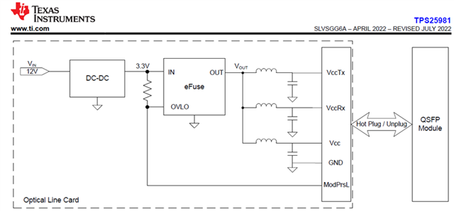
Customer is going to use TPS25981 for optical module port protection. The application scenario is similar to the following figure,

Here are two question:
1. The CR1 is must or not?
Vin spec of TPS25981 is much higher than 3.3V. Also, as checked with layout engineer, CR1/CR2 too large to place on a limited PCB size.
2. Even if a 3.3V TVS is placed next to Vin, when SCP occurs, will the Vin high voltage trigger XP3R3V_IN sources‘(I mean the 12in to 3.3V DCDC ) OVP?
And, could you pls help review the schematic? Thanks!

Regards,
Hailiang

