This thread has been locked.

If you have a related question, please click the "Ask a related question" button in the top right corner. The newly created question will be automatically linked to this question.

TPS548D22: Output noise / unstable in TPS548D22

Part Number: TPS548D22

Hi Sir,

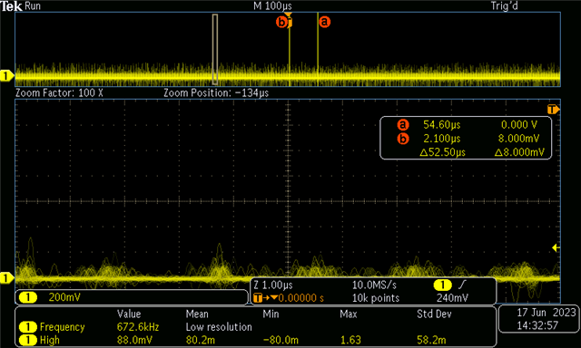
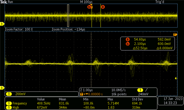
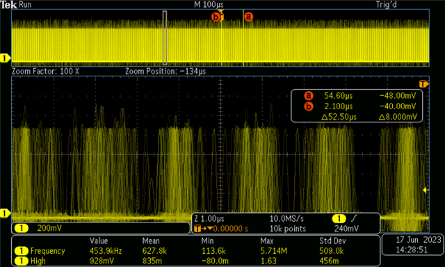
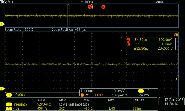
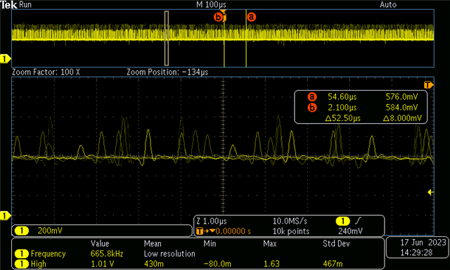
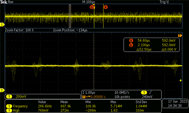
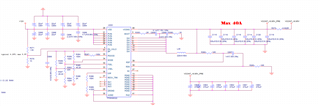
 My customer use TPS548D22 for 0.85Voutput , 40A application with FPGA. Please check the attached circuit and waveform in light load.

https://drive.google.com/drive/folders/1I2gkKqkCKEj3i4JOz7W94IiMy7uBwnoj

1. Is the waveform looks ok? Any design issue on their circuit?

2. When the load is on, Vout will down to 0.6V and FPGA will not work correctly. Any comment or testing for customer?

Thanks for your kindly help.

Best regards,

Gary Teng

  •  

    Other than over-current, I don't see any reason the output should drop down to 0.6V, and with 154kΩ from ILIM to GND, the current limit should be well over 40A.

    I don't see anything significant in the oscilloscope movie that you sent, other than some switch transition noise.

    Looking over the design, there is a lot of electrolytic/polymer capacitance, but it's hard to estimate it's impact on the loop without knowing it's ESR.  Still, based on the current design, would suggest trying to remove 2 or even 4 of the bulk output capacitors.  The loop bandwidth with just the 6 100μF capacitors is a bit high, so I wouldn't remove all of them, but removing a couple of them might help the lower frequency performance.

    Do you have an electronic load that you can slowly increase to determine if the converter is having an issue at any load, or just at the full load of the FPGA, or maybe even just at it's start-up load?

    Are you measuring 600mV at the output of the TPS548D22 or at the load?

  • Hello,

    #1. I have removed almost all the extra capacitors on the output, but the output voltage is still close 0.6V.

    #2. I measured the voltage levels at both at the load & TPS548D22 sides, but the voltages are all around 0.6V.

    #3. I also read the 0.85V voltage levels using FPGA, and the readback values are around 0.6V too.

    Any suggestions?

    Thanks.

    BR

    YC

  • Pick a single ground point on your board, can by any point, we just need a common voltage reference.  Connect the negative terminal of a voltage meter to that point.  Now measure the following points with the positive terminal of the voltage meter and record them.

    1) PVIN

    2) VDD

    3) VSEL

    4) ILIM

    5) AGND

    6) PGND

    7) RSN

    8) RSP

    9) SW

    10) VOSNS

    11) VCC_INT_+0.85_Pre at the terminal of the inductor

    12) VCC_INT_+0.85 at the terminal of R372

  • 1) PVIN : 12V

    2) VDD: 12V

    3) VSEL: ~1.2V

    4) ILIM: ~0.6V

    5) AGND: ~0V

    6) PGND: ~0V

    7) RSN: ~0V with some ripples

    8) RSP: ~0.6V with some ripples

    9) SW: spike ripples, see picture

    10) VOSNS: ~0.6V with ripples

    11) VCC_INT_+0.85_Pre at the terminal of the inductor: ~0.6V with huge spike type ripples, see picture

    12) VCC_INT_+0.85 at the terminal of R372: ~0.6V with much smaller ripples, see picture

    RSNRSPSWVCC_INT_+0.85VCC_INT_+0.85_PreVOSNS

  • It looks like there is some very severe spikes on VOUT corresponding to the switch node transition.

    I don't see the switching node, but I would recommend looking at the grounding of the TPS548D22 and the output capacitors.

    You could try increasing C897 from 1nF to 6.8nF to improve it's filtering effect at the frequency of those high spikes.

    A view of the switching node at 200ns / division might help see if something is going on there, but the voltages are checking out for what should be 0.85V output at 650kHz switching.