This thread has been locked.

If you have a related question, please click the "Ask a related question" button in the top right corner. The newly created question will be automatically linked to this question.

LM5069: Design parameters for Pulsed current

Part Number: LM5069
Other Parts Discussed in Thread: TPS2663, CSD19502Q5B, TPS2490

Hello.

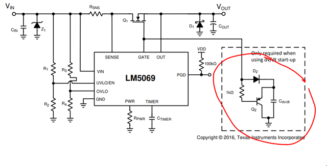
We are planning to use LM5069 in a configuration as below:

- Input voltage nominal = 50V

- Max load current (Pulsed current, 1ms pulse width with 20% duty cycle) = 12A

- Output capacitance = 1000uF

- Max ambient operating temp = 75C

- Need reverse polarity (not through schottky Diode but through MOSFET itself to minimize the IR drop)

- UV/OV protection at 48V/52V

dv/dt start up needed to manage power limit at start-up

TVS protection at input of the device.

We have checked the LM5069 design calculator. But we are not able to ascertain the correct MOSFET selection with this pulsed current, to meet the junction temp and SOA. Once the MOSFET is fully ON, the pulsed load current shall be applied as listed above.

Can you please help on this?

  • Hi Gaurav,

    Please share the design calculator for review.

    What is the current limit you set ? Can you also look at TPS2663 https://www.ti.com/lit/ds/symlink/tps2663.pdf 

    TPS26631 provides 6A continuous and 12A pulsed current support for 25ms.

    Best Regards,

    Rakesh

  • Hi Rakesh,

    Please see attached the calculator filled as needed. The FET under consideration is https://toshiba.semicon-storage.com/info/TK7R7P10PL_datasheet_en_20210127.pdf?did=60584&prodName=TK7R7P10PL

    Note that the max package that can be accommodated is DPAK. Ambient max will go upto 70C, and no air flow.

    Regards

    GauravLM5069 Design Calculator with FET Recommendation_AT.xlsm

  • Hi Gaurav,

    TK7R7P10PL is not able to survive the stress during startup and fault modes. Please select stronger SOA FET.

    Best Regards,

    Rakesh

  • Hi Rakesh,

    There shall be no active load at start-up, only the capacitive charging. I think this can be met with dv/dt delay on the Gate pin.

    During active operation, the pulsed current shall be applied. This is where we are having limitations on the FET due to size allowed in design as 2 back-back FETs are needed. Can you suggest the SOA values that the FET should meet to survive the 12A pulses?

    If we just need supply reverse polarity protection, and not load reverse current protection, can we avoid using 2 FETs (without schottky diode usage).

    Regards

    Gaurav

  • During active operation, the pulsed current shall be applied. This is where we are having limitations on the FET due to size allowed in design as 2 back-back FETs are needed. Can you suggest the SOA values that the FET should meet to survive the 12A pulses?

    Rakesh-> There is no question of SOA topic in normal operation supporting 12A pulses. SOA matters only in fault mode such as output short circuit, startup with heavy load

    If we just need supply reverse polarity protection, and not load reverse current protection, can we avoid using 2 FETs (without schottky diode usage).

    Rakesh-> Back-to-back FET configuration needed for reverse polarity protection

    Best Regards,

    Rakesh

  • Hi Rakesh,

    Our LM5069 circuit is in test now with following configuration:

    Load is 50V/5A, Output cap on drain = 400uF

    PWR pin Res = 33K

    Timer Cap= 0.01uF

    MOSFET used is CSD19502Q5B (TI). Gate has a dv/dt RC circuit of 100Ohm+0.1uF.

    Circuit seems to work ok, but there is a strange issue. When the circuit is switched off, the MOSFET still shows the source to drain short. There is a trickle voltage (~1.5V)/charge that stays on the gate pin. Once this charge is removed manually, the short goes away.


    As per IC datasheet, the 2mA internal pull down should remove any gate charge but may be its not sufficient to drain out the entire charge. Can you help here?

    Regards

    Gaurav

  • Hi Gaurav,

    Looks like 0.1uF is not getting discharged completely. Please use dv/dt circuit as shown below. Q2 helps to discharge 0.1uF quickly 

    Best Regards,

    Rakesh

  • Hi Rakesh,

    That would need considerable rework on the PCB, given that they are under test now. Is it possible to have any other option like a discharge resistor , subject to the max gate sourcing capability?

    We did not face this issue in an old design which had TPS2490.

    Regards

    Gaurav

  • Hi Gaurav,

    Can you share test results of VIN, GATE, VOUT, GATE-SORUCE (use math function) under the test condition you mentioned.

  • Hi Rakesh,

    Please see attached. The condition is captured when the circuit is switched off.

    The input Vin is not captured here (I use a 2-ch scope), but I checked separately and it follows the source voltage with a diode voltage drop through the FET body diode.

    The waveforms (both gate and source) showly decays down to zero as the capacitive load on the output discharges.

    However, if I do not connect the oscilloscope probe to the gate pin, the voltage on the gate stays at around 15-20 V (this is the case where FET IN and OUT show short or varies around 1kohm - Ideally it should go back to MOhms). Again, it decays as soon as I probe (see the second waveform).

    Regards

    Gaurav

  • Hi Gaurav,

    Let me check and get back to you 

  • Hi Gaurav,

    During turn-off event, GATE follows VOUT by a diode drop through the internal VGS clamp diode.

    If this is a concern, you have to add discharge circuit at the VOUT and check if it meets your requirement.

    Best Regards,

    Rakesh

  • Hi Rakesh,

    We tried with output discharge, but the issue remains. The gate pin retains the charge, thus keeping the mosfet source-drain path shorted.

    Regards

    Gaurav

  • Hi Gaurav,

    During turn-OFF, the GATE is pulled low by 2mA sink. So, we don't expect any charge to stay on the GATE pin. Please check whether Vout is fully discharged. 

    Can you remove Cout and dvdt capacitors and test  once.

    Best Regards

    Rakesh

  • Hi Rakesh,

    We cannot remove the output cap, its a must for our application. Also, if I remove the dv/dt cap it causes power limit to activate due to the Cout inrush at start-up.

    I have 2 options -

    1) Reduce the dv/dt cap to cater to both required slew rate, as well as decrease the gate charge during power off.

    2) Implement the pnp discharge circuit as given in datasheet and also suggested by you. In this case, please let me know the ratings of the diode and the PNP (Gate charges upto ~62V, and dv/dt cap is 0.1uF).

    Regards

    Gaurav

  • Hi Gaurav,

    For pnp discharge circuit

    Diode 1N4148W-7-F

    PNP is MMBT5401LT1G

    Best Regards

    Rakesh

  • Hi Rakesh,

    For this particular case of back to back FET with LM5069 to support 50V, 12A pulsed load (1ms ON, 4 ms off), we have now chosen the D2PAK package mosfet part IRFS4010TRLPBFCT (N-CH/100V/180A). These will be used back-back with common source. Can you confirm now that this FET should be ok in our required configuration?

    Regards

    Gaurav

  • Hi Gaurav,

    Please use design calculator https://www.ti.com/lit/zip/snvu050 to check the FET suitability

    Best Regards

    Rakesh

  • Hi Rakesh,

    We implemented the PNP discharge circuit on gate of LM5069 as suggested by you, and it works fine. However, MMBT5401 has a max rating of -5VDC for V(EBO). Wont this be violated when the PNP turns ON at power off condition, with the IC pulling the BASE pin down?

    Regards

    Gaurav

  • Hi Gaurav,

    While base is pulling down, the PNP turns-ON and discharges the Cdv/dt capacitor. In this process, we won't see violation of V(EBO) spec.

    Best Regards

    Rakesh