This thread has been locked.

If you have a related question, please click the "Ask a related question" button in the top right corner. The newly created question will be automatically linked to this question.

LM63615-Q1: Input section burned

Part Number: LM63615-Q1

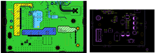
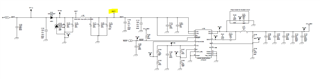
In the attached circuit input side is burned along with L100 ferrite bead on the few samples. What could be the reason for burning the parts on the input side alone? Output side of the buck regulator we are getting high impedance between output to GND 

Thanks and Regards,

Arumugam.P

  • Hello

    Under what conditions do you see the damage ?

    What is the input voltage during the test ?

    How are you applying the input voltage during the test ?

    Can you put a 'scope on the input to determine if any overvoltage spike is occurring ?

    Please provide images of your PCB layout.

    Thanks

  • Under what conditions do you see the damage ?

    ARU: Failed randomly in field in vehicle running condition 

    What is the input voltage during the test ?

    ARU: operating through 12V battery ( Min 8V, Typ 12 and Max is 16VDC)

    How are you applying the input voltage during the test ?

    ARU: During vehicle running condition the burnout is happen randomly 

    Can you put a 'scope on the input to determine if any overvoltage spike is occurring ?

    ARU: In bench level we are not seeing any over voltage and inrush current ; Vehicle level yet to be captured and analyzed 

    Please provide images of your PCB layout.

    ARU: Please refer below Layout file

    Thanks and Regards

    Arumugam.P

  • Hello

    The input capacitors will need to be closer to the VIN and GND pins of the device.

    Specifically C112 and C104.

    In general, try to avoid the use of thermal reliefs.  Use direct connections

    to power pins, components, and planes.  This includes VIN, SW, GND, Cin, Cout, Cvcc, Cboot, and L.  Thermal reliefs will add unnecessary inductance that can cause unexpected device behavior.  At the very least increase the tab width of the thermal reliefs to lower the connection inductance.

    The VCC capacitor must have a low impedance path to the GND of the device.  More ground vias around the VCC capacitor would be helpful.

    Thanks

  • Hello

    I will close this post due to inactivity.

    Thanks