This thread has been locked.

If you have a related question, please click the "Ask a related question" button in the top right corner. The newly created question will be automatically linked to this question.

TPS22975: Used as an inrush current limiter

Part Number: TPS22975
Other Parts Discussed in Thread: TPS22967, TPS22953

Hello Team,

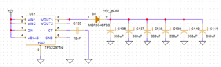
I am using the TPS22975N as an inrush current limiter. It is used to charge a big capacitor (2,000 µF) used as an energy tank for our system.
This design have been made following all chip recommendations but CIN/CL which should be greater than 10. As a matter of fact, CT is set to 10 nF which limits the current to less than 900 mA at any moment: this current can easily be provided by our primary power supply block.

Do you confirm our assumption is correct ?
Do you detect any flaw in our schematic ?

To finish with, at power-up there is a transient state during which (Vin-Vout).Iout rises up to 2 W for 10 ms or so. I haven't found the usual power transient derating curves in the datasheet: can the component handle such a peak for this little time ?

Thanks in advance for your reply, regards,

Mathieu

  • Hi Mathieu, 

    Some schematic comments:

    • Typically we recommend Cin>Cout but this really has more to do about the stability of your voltage rail. The input capacitance will hold up and stabilize the input rail during high current draw events such as turn on. Therefore, depending on if the supply has a sufficient power capability, input capacitance might not be needed.
    • Another concern with Cout>Cin is potential reverse current flow when Vout > Vin, however the diode you've put on Vout should protect against any reverse current flow to Vin. 
    • With regard to sequencing, one thing to consider since you are tying VIN,ON, and Vbias together, is if you are ever pulling ON high when Vin/Vbias is low, we want to be sure Vbias is at least 2.5V tD (ON delay time) after Von is at 50% to be sure the device is biased correctly.

    With regard to your concern of 2W dissipation, we specify this device for max 6A continuous current and do not specify any transient SOA curves.

    We additionally do not have a max output capacitance rating.

    Section 10.2.2.1 "Inrush Current" of the datasheet will allow you to calculate your maximum inrush current given your output capacitance and slew rate. A slower slew rate would be preferable since it would lower your inrush current as you've mentioned to less than 900mA. There additionally is no hard limit on CT. However, the only limitation is that a longer turn on time could cause the device to heat up.

    Best Regards, 

    Elizabeth 

  • Hi Elizabeth,

    Thank you very much for your (quick and) comprehensive reply Relaxed.

    Let me ask you some clarifications though:
    - The MBRS340 diode can have a reverse current up to 2 mA max at high temperature, will the TPS22975 withstand this reverse current?
    - I am afraid I don't understand your "when Vin or Vbias is low, make sure that Vbias is at least 2.5 V after Von is at 50%"; since all three signals are tied together, there shouldn't be any problem, should it?
    - 2 W dissipation: even if there is not SOA curve, do you think the TPS22975 can withstand such a power during 10 ms or so without lowering the chip's MTBF? Since TPS22975 and TPS22967 have the same package (WSON8) and the same dissipation ability, could I use the SOA curve given in the TPS22967 datasheet (see below)? In this case there should be no problem to guarantee a 70 kh lifetime roughly. What is your opinion about this point?

    To finish with would you advise me to use another current limiter chip TPS22xxx (or any other) to make sure the design will be reliable?

    Best regards,

    Mathieu

  • Hi Mathieu, 

    We do not stress test or characterize the internal body diode of the FET so we would not recommend using our devices bidirectionally, and I cannot say whether the device would be affected by a 2mA max reverse current at high temperatures since we do not characterize this. 

    I would recommend looking at another inrush current regulated load switch with integrated reverse current blocking when disabled and without quick output discharge: for example, the TPS22953. This device additionally has power good, thermal shutdown, and under voltage lock out. 

    More information can be found here: 

    https://www.ti.com/lit/ds/symlink/tps22953.pdf?ts=1686177622682&ref_url=https%253A%252F%252Fwww.ti.com%252Fproduct%252FTPS22953

    We do not specify a SOA curve for the TPS22975, however we do support up to 6A of continuous current. Although the device will heat up as the slew rate is being controlled, thermal shutdown will also protect the device against any damage which could be caused by heat. 

    Best Regards, 

    Elizabeth 

  • Hi Elizabeth,

    I understand your point of view and I will follow your advice: design a system based upon TPS22953 for example.
    I you agree I'll submit the new schematics when done.

    Thanks for your help.

    Mathieu