A related question is a question created from another question. When the related question is created, it will be automatically linked to the original question.
If you have a related question, please click the "Ask a related question" button in the top right corner. The newly created question will be automatically linked to this question.
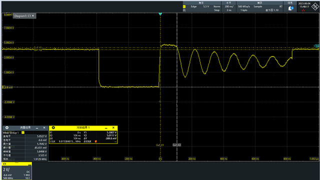
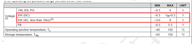
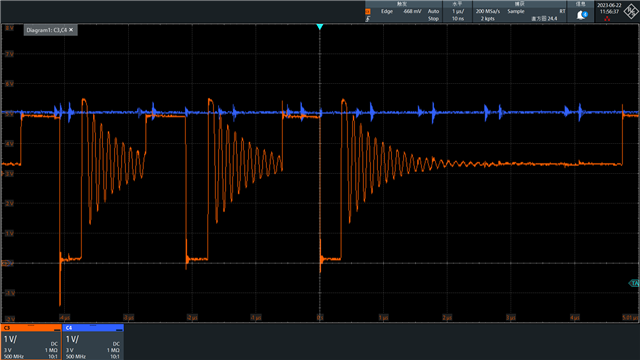
The customer test the wave of SW with Vin at 5V. The find the SW voltage(5.7V) is more than 5.3V lasting 102 ns, which is longer than the time in datasheet . They want to know whether it could damage the device.
Can you please provide me the measurements of input voltage(across the device input capacitor) and the SW node voltage using 1V/div in same scope plot.
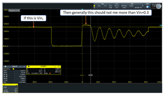
I suspect the Vin is high that's the reason I am asking VIn and SW node voltage with 1V/div to make things clear. So can you please provide me the measurements of input voltage(across the device input capacitor) and the SW node voltage using 1V/div in same scope plot.
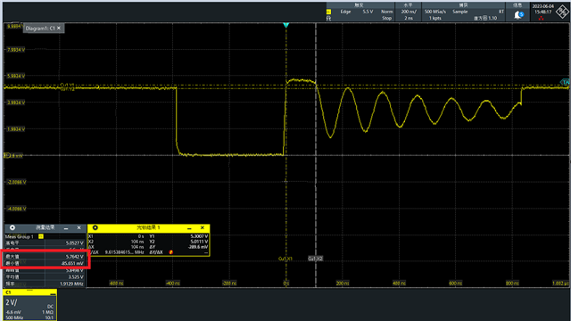
Now it looks like, Vin is around 5.1V and SW the peak is around 5.4V. There should not be any concern, but just to make sure about the layout, can you please share the customer layout, sometimes the peak of SW also depends upon the SW plane area and the measurement setup.
Yes, you are correct and this amplitude of the ringing and the frequency of ringing is also depends upon the SW plane area in the layout as it adds the parasitic inductance.
If you don't have any further questions, can you please close the thread by clicking on resolved.