A related question is a question created from another question. When the related question is created, it will be automatically linked to the original question.
If you have a related question, please click the "Ask a related question" button in the top right corner. The newly created question will be automatically linked to this question.
The schematic looks good. I notice the PCB Document has 4 copies of what I think are the same layout for each IC? Is that correct?
One concern is the EN trace running alongside the VBST node. This is not recommended because we do not want the enable pin to couple to high noise. Customer could use a VIA to go to another plane and then come back out where the enable resistors are. This would also allow the customer to move the PGOOD resistor closer to the PGOOD pin, as recommended by the datasheet.
Frankly, I feel like the customer could move all of the components a little closer to the IC. They are allowed to use 0402 size components unless stated otherwise in the layout section of the datasheet. If 0603 is a hard requirement, then I suppose this is as good as the layout is going to get. Please make sure they understand my concerns about noise coupling on the EN pin from the SW and VBST.
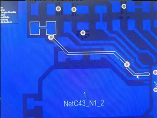
Going thru a VIA as you showed is good. but I can not tell what underneath that trace, but just make sure to use internal layer(s) as ground plane(s) and shield that trace from noisy traces, power traces and components.