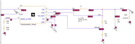
This thread has been locked.

If you have a related question, please click the "Ask a related question" button in the top right corner. The newly created question will be automatically linked to this question.

TPS629206: About PSPICE Simulation Results

Part Number: TPS629206


Hi TI engineer,

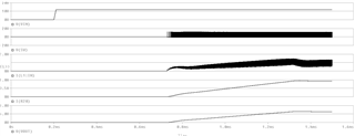
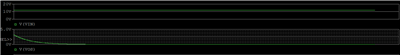
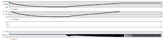
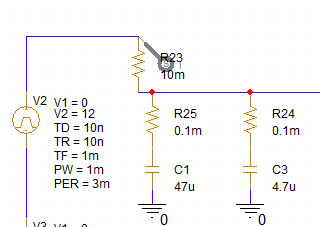
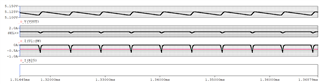
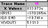
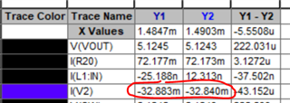
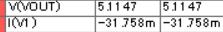
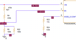
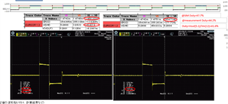
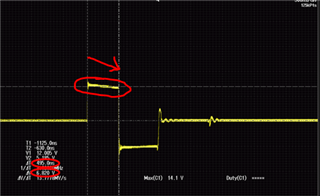
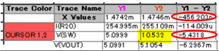
I am simulating using a PSPICE model with input voltage of 12vDC and output voltage of 5vDC, but the output voltage is not 12v, is there something wrong with the settings as this is my first time using PSICE?

I have confirmed that the output voltage is 5V in the actual circuit on the board.

  • Hi Onishi,

    Your simulation result looks strange.

    I have the same setup and the results are as below. The output voltage is normal 5V.

    Could you please attached the simulation waveforms as mine?

    BTW, the frequency you choose is 1M and the inductor is 3.3uH. The inductor current ripple can be calculated as (Vin-Vout)*Vout/Vin/L/fsw=0.884A. Also the output current you set is 5/(3.3/0.6)=0.91A, but TPS62906 is a 600mA part. It may trigger the Over Current Protection so I don't recommend you to use 3.3uH inductor under this application.

  • Hi TI engineer,

    Thank you for your research.

    To begin with, is the VIN power supply DC correct?
    In the graph you gave us, there is a delay, so are you using a pulse power supply?
    But the waveform looks DC.
    I am not sure where the 1MHz setting item is located, so could you please tell me?

    I will also attach the waveform.

    It may be difficult to see without knowing how to change the background color. Sorry.


    As for the output current, the load never flows 600mA in actual operation. Thank you for your suggestion.

  • Hi Onishi,

    Yes, I used a pulse power supply.

    Actually I just used the PSPICE for TI model of TPS629206 at ti.com and change the resistors as below files.

    TPS629206_PSPICE_TRANS.zip

    You can try to run this simulation and see what's the differences.

    Did you edit the simulation setting? You can directly send the simulation files to me.

    As for the frequency, you choose 11k+6.8k=17.8k Mode resistor, so that the frequency is 1MHz per datasheet.

    Still we should pay attention to the inductance choice. Usually we'll set the inductor current ripple within 40% of the rated current. You can let me review your schematic then.

  • Hi TI engineer,

    Thank you very much.

    I used the same model as the one you gave me and changed the resistor values and configuration for the simulation.
    So the simulation settings are still the same.
    However, I have changed the VIN power supply to DC and the simulation is not working properly.

    Is the pulse power setting the same as the model's default setting?
    I will try that.

  • Hi Onishi,

    The default setting is a pulse source of input volateg.

    I just tried a DC supply and the simulation fails, too.

    This may due to the initial setting of this simulation model, so please using the default DC pulse voltage source and try again. 

    Thank you!

  • Hi TI engineer,

    I am using PSpice to monitor current,

    If you know the cause, please let me know.
    The measurement point is the V1 point shown in the attachment.
    The current value does not change when I change the load.

    The attached graph is for a load of 71Ω, input voltage = 12v, output voltage = 5v.

  • Hi TI engineer,

    I would like to add something to my earlier explanation, as it was insufficient.

    What I wanted to tell you is that the input current (current from V1) is low,
    I wanted to tell you that the input current (current from V1) is low and does not change even if the load resistance is changed from 71Ω.

    Please let me know if you can provide any clarification.

  • Hi Onishi,

    That's because the simulation is so ideal that the input current is pulse when High-side FET on and very low when High-side FET off.

    What you measured is the High-side FET off current, so it's not related to the loading. 

    You can zoom in the input current and see it equals the inductor current when SW is high.

  • If you want to detect the mean value of input current, you can add some non-ideal resistors/inductance of the input trace and try again.

  • Hi Athos,

    Thank you very much.

    I understand that current flows when the high-side switch is turned on.

    However, the input current (current from V1) is negative,
    Also, if the load resistance is 71Ω,
    Is it correct to calculate the input current using the following formula?
    The loss is not included.
    Iin=V2*I2/η*V1=32.7mA
    V2=5v
    V1=12v

    Sorry for the rudimentary question.

  • Hi Onishi,

    The negative current is due to the direction of the current probe, no need to confuse about it.

    You calculation is right, η is the efficiecy.

    The mean value of the input current in the simulation should be following this.

  • Hi Athos,

    Is the average correct by reading the cursor values in the attached graph?
    Or is there another way?

  • Hi Onishi,

    To get the mean value, you can use a higher input resistance, such as 1Ohm and monitor the current at steady state.

  • Hi Athos,

    We were able to reproduce it here as well.
    Thank you very much.

  • Hi Athos,

    Please let me know if there is a method or calculation formula for setting the hysteresis between the UVLO detection voltage and the released voltage.
    In the current simulation, it seems to have a hysteresis of about 2V.

    Also, the datasheet states 200mv at the tipical.

  • Hi Onishi,

    The UVLO is not only determined by VIN but also by voltage of EN since you have a divider resistors between Vin and EN.

    In you simulation, the rising threshold is 1/90*(90+470+430)=11V and the falling threshold is 0.9/90*(90+470+430)=9.9V.

    The hysteresis is 1.1V.

    To calculate the UVLO hysteresis, if you use a divider for EN, you can use 0.1V / Rbottom * (Rbottom + Rtop).

    If EN remains high, UVLO is determined by Vin and the hysteresis is 200mV.

  • Hi Athos

    I now understand that both rise and fall are determined by the resistance values of EN and VIn.
    Thank you very much.

  • Hi Athos,

    What is the output of the SW terminal?

    We measured the board and obtained waveforms with PSpice simulator,
    Duty was calculated.

    The PSpice simulation waveform showed 47.7%.
    The measured waveform on the board was 44.2%.
    The output voltage was 5.1v for both measurements,
    The calculated value would be Vout(5.1)/Vin(12)=41.6%, right?

    Is this result discrepancy within the normal range?

  • Hi Onishi,

    Athos is on public holiday, will reply you on 6/25.

  • Hi Onishi,

    The output of SW is the PWM of the Buck output.

    Actually, the duty= [Vout + Iout * ( Inductor_DCR + Rdson) ] / Vin. It's higher than Vout(5.1)/Vin(12)=41.6%.

    Your measured waveform is reasonable because the input is not stable at 12Vdc. You can see there's voltage drop of SW when High-side MOSFET on.

    In your simulation, the SW max is 10.532V so the duty D=5.1/10.532=48% is also normal.

    This thread is already 13 days. Please build a new thread if you have new questions not related to the original one, thank you!

  • Thank you very much.
    I understand that there is no problem.

    I will also make sure to start a new thread for future questions.