This thread has been locked.

If you have a related question, please click the "Ask a related question" button in the top right corner. The newly created question will be automatically linked to this question.

TPS40345: Output ripple improvement inquiry

Part Number: TPS40345

Hello,

My customer is using the TPS40345 as FPGA core power supply.

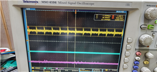
Below is the output ripple capture image. The measured output ripple characteristic is significantly worse than guided by the datasheet.

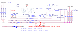
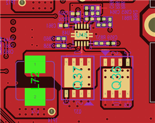
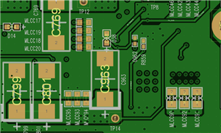
Below are the customer design files and inductor datasheet.


LPMT6530-1H Series DataSheet_210219 (1).pdf

Q1 ) Please review whether there is a problem with the design of the TPS40345.

Q2 ) Please advise on how to improve the output ripple characteristics.

Thank you.

JH

  •  

    Q1 ) Please review whether there is a problem with the design of the TPS40345.

    No, there is nothing wrong with the TPS40345 that is creating the very high frequency (10s to 100s of MHz) noise spikes on the output voltage.

    Those spikes may be real or a measurement artifact of the oscilloscope and probe, and its attachment to the PCB.

    Q2 ) Please advise on how to improve the output ripple characteristics.

    To minimize noise artifacts from the oscilloscope probe: 

    Connect oscillscope grounds to only 1 ground point on the board under test

    Measure Vout using a "tip and barrel" method with a very short ground loop as far from the inductor as possible (ideally on the opposite side of the PCB)

    If the noise is real, it is likely ringing on the switching node coupling around (or through) the inductor to the output capacitor and then not being removed at the output due to the capacitor and layout ESL.  Looking at the component selection and the component layout, there are likely a number of improvements that can be made.

    1) Improving ringing at the switching node

    One component change with the existing layout that can help reduce switch-node ringing and thus its coupling to VOUT is the series BOOT resistor.  Currently 2Ω, that could be increased to 4.7Ω to reduce the rising slew-rate on the SW node and thus the ringing.

    Another component would be to replace one of the Input and Output capacitors with a 2.2-10nF capacitor whose self-resonance frequency is matched to the ringing frequency observed on the switching node. That would help reduce the input and output impedance at these high frequencies while allowing the capacitor to be self-damping.

    There are also a number of layout improvements that could be made.

    1) The feedback sense trace that is currently routed on the backside of the PCB between the high-side and low-side FETs could be routed around the bottom and right side of the MOSFETs to avoid separagting the ground between the MOSFETs and increasing the loop-length for the high-side drain to low-side Source bypassing

    2) The high-side Drain to low-side Source Bypassing, currently on the bottom of the board could be split to place half on top and half on bottom, oriented horizontally instead of vertically.

    3) The Drain Tab vias on the high-side FET could be reduced and respaced to allow the ground pour on the bottom layer to fill between the vias to re

    4) Additional vias could be added to GND side of the output capacitors to reduce their inductance back to ground

    5) The vias in the drain tab of the low-side MOSFET should be eliminated along with any internal plane connected to the SW node.

    6)  You can increase the copper pour to copper pour spacing between the SW net and the VOUT net to reduce the high-frequency capacitive coupling from the SW not to the VOUT node

    d7) Adding an RC snubber or high-speed rectifier diode from SW to VIN between the low-side and high-side MOSFETs can also help reducing the ringing  energy at  the switching node to reduce ouptut voltage noise.

    8) Adding small 2.2-10nF 0404  capacitors from VOUT on the TOP to GND at the source of the synchronous rectifier would help remove the high-frequency noise before it can pass through the vias