This thread has been locked.

If you have a related question, please click the "Ask a related question" button in the top right corner. The newly created question will be automatically linked to this question.

BQ25886: Please review the schematic, and have few questions

Part Number: BQ25886

Dear TI experts,

My customer drew their first schematic with BQ25886. Could you review the schematic first?
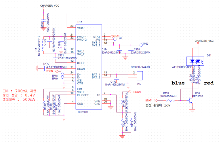
and here are more questions ;

1. my customer will not use thermistor. Is it okay to float TS(7) pin? or just connect resistors like the schematic above?

2. My customer will not use OTG pin. Is it okay to connect OTG pin to GND? or use specific value of resistor?

3. My customer will always active BQ25886. How about \CE pin? datasheet says \CE pin is internally pulled low with 900kohm resistor. in this case, Can I just float \CE pin? 

4. My customer also will not use USB communication, only will use 5V adapter. In this case, is it okay to float D+ and D- pin?

5. Is PG pin only indicates about input source, not charging/discharging status? then my customer will not use PG pin, as float. please confirm it.

Best regards,

Chase 

  • Hi Chase,

    My schematic review is as follows:

    1. I see OTG is disabled because OTG is pulled low.

    2. Input current limit is 694 mA.

    3. Charge voltage regulation us 8.4 V.

    4. Charge current regulation is 499 mA.

    5. Correct me if I am wrong, but you want 2 LEDs to monitor the STAT pin? Typically we just pullup the STAT pin to VREF with a LED and 2.2 kOhm resistor. LED ON means STAT open drain is conducting and LED OFF means STAT open drain is not conducting.

    I will answer the questions in order.

    1. If the customer does not wish to use thermistor, permanently bias the TS pin between T2 and T3 as shown in the EC table. This is roughly between 68% and 45% of REGN.

    2. OTG to GND is ok.

    3. Please pull CE/ to GND to charge.

    4. As shown in Section 8.3.3.2, "The charger input current is always limited by the lower of ILIM pin or input source detection." Therefore I would short D+ and D- together to simulate a DCP (3A) and the customer's lower 700 mA ILIM setting will be the input current limit.

    5. You are correct PG pin only indicates good input source. STAT can indicate charge in progress, charge complete, charge disabled, and faults.

    Regards,

    Mike Emanuel

  • Dear Mike,

    Thank you for your support.

    Here are more questions from customer.

    1. Could you recommend the value of vias resistors of TS pin?

    2. about LED, my customer want to light red LED if the stat pin is low (charging), and green led on if the stat pin is high (charging complete, because of Q50 TR.) Please check this schematic.

    (added question)

    3. They want to use SYS pin when VBUS is applied.

    3-(1) Is it okay to tie BAT and SYS pin? (and connect it to other IC?)

    3-(2) if not, Is it okay to connect only SYS pin to the IC which need 8.4V voltage, not connect BAT pin to the IC?

    3-(3) How can I change the value of SYS voltage?

    Best regards,

    Chase

  • Hi Chase,

    1. I would program the TS pin to 60% of REGN, use a 6kOhm for the bottom resistor and 4 kOhm for top resistor. Use higher resistors if you are worried about the leakage on the system.

    2. I understand. Please test according to your application.

    3-(1) No you should not tie BAT and SYS. The battery and system load must be separated by the BATFET.

    3-(2) The minimum system voltage is 6.2 V. That means if the battery is below 6.2 V the system will be regulated to 6.2 V. If you need 8.4 V on the SYS pin and the battery is below 8.4 V you will get whatever the battery voltage is. Please read Section 8.3.6.1.

    3-(3) The value of the SYS voltage is fixed at MINSYS of 6.2 V or slightly above the battery voltage if above MINSYS.

    Regards,

    Mike Emanuel