Hi David,
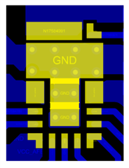
Hope you meant to connect it like this four ground pins together as a shape in the layer where IC is going to place. Please correct me if I am wrong:
Original question:

Hi David,
Hope you meant to connect it like this four ground pins together as a shape in the layer where IC is going to place. Please correct me if I am wrong: