Sir
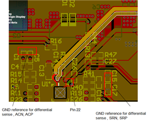
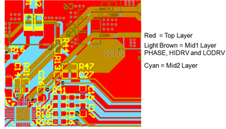
We are executing the PCB layout, the brief routing plan is as follows
Top Layer (Placement): IC and other components referring to AGND
Mid1 Layer: AGND and routing
Mid2 layer: PGND
Bottom Layer: (Placement): MOSFETs, Rsense, Inductor, Input and Output capacitors (Intended path for high-current carrying)
For a complete PGND plane, we plan to route PHASE, HIDRV, and LODRV in the mid1 layer
Could you please recommend whether the traces mentioned above is essential to be shielded or not?
Thanks
Regards
Ben