This thread has been locked.

If you have a related question, please click the "Ask a related question" button in the top right corner. The newly created question will be automatically linked to this question.

UCC28070A: RIMO Selection with DC Offset at CSA/CSB

Part Number: UCC28070A
Other Parts Discussed in Thread: UCC28070

Hello,

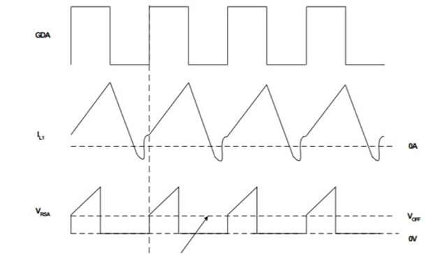
UCC28070A's data sheet has Equation (18) to select RIMO value. But if a signal voltage at CSA and CSB pins has DC offset, does it have an effect on the Equation (18)? I'm wondering if I need to subtract the DC offset from the equation, for example.

Best regards,
Shinichi Yokota

  • Hi Shinichi-San,

    Thank you for the query on UCC28070.

    The DC offset is generally limited to between 100mv - 150mv (200mv max). It does not have any effect on equation 18 on selection of Rimo resistor. 

    The  offset adds a small DC error signal to the CSA and CSB signals. It is just a DC voltage that stops gate drive that would otherwise would result due to an erroneous current transformer signal. The effect of this offset is to add a "dead zone" around the zero crossing.

    During this time when Rsa is below Voffset (the DCM time mentioned in the datasheet) the gate drive may go to full on because the sensed current is zero and the error amp has a finite output. This may saturate the current amp and cause large spikes of current around the zero crossings. Adding an offset on CSA/CSB prevents these large current spikes and generates a dead zone. This is mainly having effect at zero crossings where at low line voltages the current transformer cannot sense an adequate line current because the current into the CT is is so small and parasitics and ringing cause measurement error.

    Overall no need to make any changes to the equations.Please let us know if you have further questions.

    Regards,

    Harish

  • Harish,

    Please let me ask an additional question.

    My understanding is that an input power limit occurs when the IMO output voltage reaches the value of the left side of the Equation 18. For example, when the RIMO is 10 kΩ and the IIMO(max) is 60.3 µA, the input power limit should happen at the IMO output voltage of 0.603 V (= 10 kΩ × 60.3 µA). But, it doesn't even when the IMO output voltage goes beyond 0.7 Vrms.

    Is something wrong with my understanding?

    Best regards,
    Shinichi Yokota

  • Hi Shinichi-San,

    You are correct with the working above.

    So what what happens is as you said, when you select RIMO corresponding to the lower extreme of a voltage bin, we select maximum value of RIMO. But when there is variation of voltage and voltage reaches upper extreme of that bin, IMO current naturally increases which is why you are seeing an increase on voltage from 0.6 to 0.7V. So this has to be taken into account while designing the system and ensure that PKLMT function triggers and protects the system. So PKLMT should have enough headroom to address this and not arbitrarily be set at a high value. Please let us know if you have further questions.

    Thank you

    Regards,

    Harish