This thread has been locked.

If you have a related question, please click the "Ask a related question" button in the top right corner. The newly created question will be automatically linked to this question.

LM46000: Not possible to Enable when the temperature is > 50degC

Part Number: LM46000

Hi! I have been using the LM46000 in combination with LM2991S for a long time, but it's only recently that I have discovered an issue that I cannot explain.

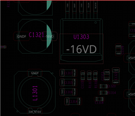
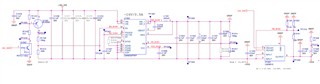
The design consists of the LM46000 in inverting configuration to generate the negative -16V. Then the LM2991S converts the -16V into -15V.

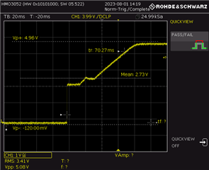
The problem appears when I try to enable the circuit shown, ONLY when the temperature around the layout area covered by the circuit is above a certain temperature (somewhere between 50-60degC). At this point, I can't do anything but wait (or cool down) until the temperature drops to 30-40degC when the circuit starts working again. Otherwise, when the temperature is low, I can enable/disable the circuit with no problems.

Important to say that:

- The LM46000 reaches 50-60degC due to casing and hotter parts close to the circuit. If the pcb is by itself the temperature never goes above 40degC.

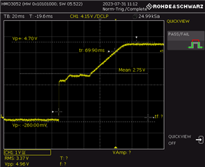
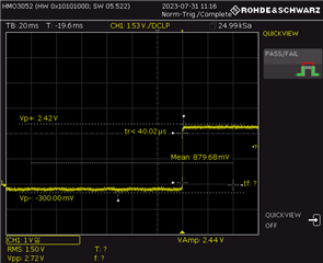
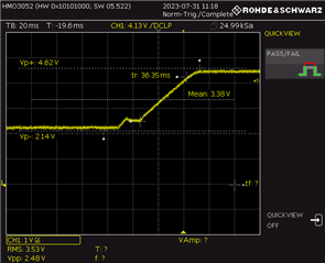
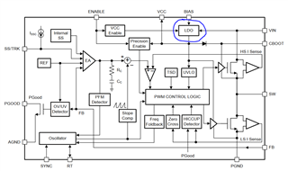
- my -16V_EN input works as expected, so I can always get a positive voltage at the enable pin of the IC. The problem is that the IC will not respond to that.

- If I enable the circuit at lower temperatures (30-40degC), it works with no issues even at 80-90degC. The issue would appear then if I disable the circuit and enable it again.

- When the IC does not work the voltages are as expected when disabled, except at the EN input of the IC.

I have tried:

- Pulling up EN pin to Vin so is always enable, at higher voltage than my current enable voltage but it does not change anything.

- Disabling the LM2991S, but the LM46000 continues showing the same problem. 

- Tested many different LM46000's concerned about the Thermal shutdown protection, but the temperature never goes as high as the threshold shown on the datasheet. (st

At this point Im very confused even about how to continue debugging this issue. I would really appreciate receiving some ideas or possible reasons that help me solve this. Thanks in advance!


  • Hi Jose,

    Please monitor the voltage between the enable and the chip ground, and perhaps investigate your level shifter. 

    If you think this is a thermal issue, please post an image of your PCB layout and well evaluate it.

    Thanks

  • Hi Daniel,

    Thank you for your reply. Attached all the screenshots and investigation made so far:

    - At ambient temperature (25-30deg), the circuit responses as expected after the disable->enable sequence. Monitoring the TP1306 (Enable pin) vs TP1303 (chip ground) I get a first step up to 2.4V followed by a second ramp up to 4.6V, as shown in Fig. 1. (the later ramp is due to the IC ground ramping from [0V] to [-16V].

    - If I heat up the circuit externally (50-60deg approx, measured with a general infrared thermometer), there is a first step up to 2.4V (same as before), but the circuit does not get enabled even though the voltage at the enable pin is the same. See Fig. 2.

    - Fig. 3 shows the second voltage ramp up to 4.6V happening only after the circuit has cooled down.

    Enable input - COLD       
                              Fig.1: 30degC                                                                              Fig.2: 50degC 


              Fig3.After cooling down 50degC -> 35degC


    I have checked the driving circuit and the outputs are as expected, but you can also see that looking at the previous figures as the EN pin goes up to 2.4V.

    Note that even if I tie the EN pin to Vin, the circuit does not start after the first step - so I discarded a low EN voltage issue.


    The circuit is placed on the bottom layer of a 10 layers PCB. Here some information:

    Bottom layer layer 4  
                                Bottom layer                                                                                 4th layer
    3 layer            
                                  3rd layer                                                                                  2nd layer
    top layer            
                                 Top layer                                                                               Top layer assembly 


    Thanks!


  • Hi Jose,

    The device sinks a very small amount of current at the EN pin. Normally this isn't an issue, but when resistor values on the 1MOhm order of magnitude are selected, then it becomes an issue.

    My suggestion would be to lower the EN resistors to less than 100KOhm max, and see if you have this issues. I'm also not sure what the reason for the BJT is and probably can be removed. Let me know if you can get the circuit to work after you implement both of those things.

    Thanks,

    Andrew

  • Hi Andrew,

    Thanks for your reply. I have changed both resistors R1728=62k and R1315=11k, keeping the same ratio. The results are unfortunally the same as in my previous message:

    Fig.4 shows the circuit working with "cold" temperature.
    Fig. 5 shows the circuit not working with "hot" temperature. The voltage at the enable pin is high, but the circuit does not turn ON.
    Fig.6 shows the circuit working around 1 min after I stop applying external heat, and the temperature reaches "cold" values.


                              Fig.4: 30degC                                                                              Fig.4: 50degC 


              Fig6.After cooling down 50degC -> 35degC


    "I'm also not sure what the reason for the BJT is and probably can be removed." :

    - I understand that you refer to the BJT pnp, Q1302. Its function is to enable the LM46000, since the EN pin is connected to the IC ground when the BJT is open. So the two cases are:


    1) When -16V_EN is high, Q1303 turns ON -> Q1302 base=13.37V ->Q1302 emitter=16V, so Vbe < 0V -> Q1302 is ON -> Enable = 2.41V respect to chip GND (which goes down to -16V when the chip is enabled).

    2) When -16V_EN is low, Q1303 turns OFF-> Q1302 base=16V ->Q1302 emitter=16V, so Vbe = 0V -> Q1302 is OFF-> Enable = 0V respect to chip GND.

    Summarizing, I cannot control the enable pin if I remove BJT.

    Thanks!

  • Hi Jose,

    Understood on the Level shifting BJT circuit.

    a collogue of mine wrote an app note on IBB's (see below), and I'm trying to see what he did differently than you. For one, he did opt to use MOSFETs instead of BJTs, but I'm going to assume that's not the issue.

    https://www.ti.com/lit/an/snvaa65/snvaa65.pdf?ts=1689267817548&ref_url=https%253A%252F%252Fwww.ti.com%252Fproduct%252FLM63615-Q1

    Does removing the soft start capacitor do anything? What does SS pin do in Hot and Cold conditions?

    Thanks,
    Andrew

  • Hi Andrew,

    Attached the tests with and without SS capacitor (C1327)

    Fig.7) SS pin (TP1301) vs IC gnd (TP1303) - COLD reset with SS capacitor - disable->enable - the circuit works

    Fig.8) SS pin (TP1301) vs IC gnd (TP1303) - COLD reset with SS capacitor - enable->disable - the circuit works

    Fig.9) SS pin (TP1301) vs IC gnd (TP1303) - HOT reset with SS capacitor - disable->enable - the circuit doesn't work

    Fig.10) SS pin (TP1301) vs IC gnd (TP1303) - COLD after being HOT reset with SS capacitor - enable-> disable - the circuit works (after cooling down)

    Fig.11) SS pin (TP1301) vs IC gnd (TP1303) - COLD reset without SS capacitor - disable-> enable - the circuit works

    Fig.12) SS pin (TP1301) vs IC gnd (TP1303) - COLD reset without SS capacitor - enable -> disable - the circuit works


                                  Fig7.                                                                                     Fig8.


                             Fig.9                                                                                             Fig.10


                               Fig.11                                                                                         Fig.12

    Thanks again for the support!

  • Hi Jose,

    Hmm, The pulses seem weird, but the device works. I have some additional questions:

    What does VCC look like when you heat up the device? Does anything funny happen after you pass the threshold?

    What does SW look like at Cold and Hot?

    What happens when BIAS is connected to IC ground (feature is disabled) instead of regular ground.

    Thanks,

    Andrew

  • Hi again,

    I'm going to skip the response two the first two questions as the voltages were the same cold and hot.

    But it seems like connecting bias to IC GND instead of GNDF has solved the issue. Slight smile So that is awesome.

    Have tested it on two boards now.

    But do you have any idea why temperatures above a certain threshold would make the original design fail to enable?

    Thanks,

    José 

  • Hi Jose,

    If I had to guess, I would say it's something about the way IBB's are configured messes with the startup of the Bias LDO. And then this affects how the device switches. It seems to work fine at room temp, but it changes at higher temperatures.

    VIN/VCC/BIAS are all different voltages. I asked to measure VCC  at hot temp as I suspected it wasn't turning on, but you confirmed that's not the case.

    Thanks,
    Andrew

  • Okay. Maybe that's the case. Slight smile

    Anyway, thank you so much. I greatly appreciate your help. You've been very thorough.

    Have a great day.

    José  

  • Hi Jose,

    You're welcome! Slight smile

    Have a great day!

    Thanks,

    Andrew