


Hi,
The customer has some questions about TPS4811-Q1, and I would greatly appreciate your response.
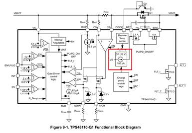
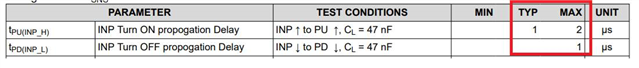
1. For INP Turn ON propagation Delay, where is the CL written in the test condition connected?
Can it be understood as the parasitic capacitance Cgs between the gate and source of the switch?

2. Is there a product similar to TPS4811-Q1 that uses a charge pump to charge bootstrap capacitor, but with a smaller propagation delay (preferably less than 300ns, customers need to use this product to complete voltage conversion within 2.34us, and the 1us delay of TPS4811-Q1 is too high)
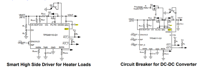
3. For a normal Bootstrap circuit, if the upper switch continues to conduct and the lower switch continues to turn off, will the voltage on the bootstrap capacitor continue to decrease due to leakage current, causing the upper switch to turn off?
Ericsson's application scenarios include the following two, hoping to have a chip with lower delay and smaller area, without the need for current sensing and other functions.
Thanks!
