Hello,
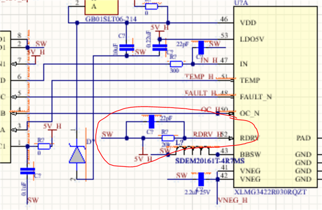
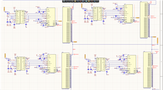
I have attached primary side of the full bridge DCDC converter. I have used the half bridge implemented in the datasheet. Could you please tell me if its correct.
Thank you in advance,
Neha Agarwal
This thread has been locked.
If you have a related question, please click the "Ask a related question" button in the top right corner. The newly created question will be automatically linked to this question.
Hello,
I have attached primary side of the full bridge DCDC converter. I have used the half bridge implemented in the datasheet. Could you please tell me if its correct.
Thank you in advance,
Neha Agarwal
Hi Neha,
For a full bridge, the two half bridge switch nodes are not directly connected. This means the sources of the high side devices are not on the same node. The high side devices then will have to use separate isolated bias supplies or will have to use bootstrap supplies to supply the 12V to VDD.
The Rdrv pin on all four devices. The pin can either be shorted to LDO5V of the device or it can be connected to the source pin of the device via a resistor. The resistor value can be chosen from Figure 7-4. Turn-On Slew Rate vs Drive Strength Resistance. The SW node cannot be connected directly to 5V_H (that is connecting LDO5V to source of the device).

Best,
Kyle Wolf
Hi Neha,
The updates made look good. The problem with the Rdrv pin still exists. Rdrv (pin 52) can either be connected to LDO5V (pin 53) via 0 ohm resistor or Rdrv (pin 52) can be connected to the device source via resistor with value chosen based on Figure 7-4. Turn-On Slew Rate vs Drive Strength Resistance from the data sheet. This change must be made on all four FETs. In addition to this, all pins labelled with VSWNET must be labelled with individual net names. This change must be made so that the pins are not connected on the layout.
Best,
Kyle Wolf
Hi Kyle,
One more question
for the isolator, what DCDC isolator would you recommend
Regards,
Neha
Hi Neha,
In the picture from the application note, R3 & R5 can not be populated at the same time. If R3 is populated then R5 must not be populated on the board and if R5 is populated then R3 must not be populated on the board.

The picture above, the latest schematic I have from you, shows a direct short from 5V_L to PGND. 5V_L is the net for the pin that produces 5V and PGND is 0V, they cannot be connected. In this situation, I would suggest deleting the node 5V_L from the wire here and leaving PGND.
For the question about the isolator. On the EVMs we use the ISO7741FDBQ. This gives us 4 channels, one into the GaN FET (for IN) and three out from the GaN FET (for TEMP, /OC, /FAULT). For testing we suggest using all of the protection features and therefor a 4 channel isolator. For production the number of channels on the isolator can be cut down by not using the protection features' output signals, the protection features will still work internally on the GaN device.
Best,
Kyle Wolf
Hi Kyle,
Also one more question, from where did the 5V_H, 5V_L, VNEG_H come
and Please see the schematic below after the changes:
Regards,
Neha
Hi Neha,
The most recent schematic looks good, the Rdrv pins look correct. For the isolated bias supply you are looking for without a transformer and bridge circuit. TI's UCC14140, is a possible solution. It works by integrating the necessary transformer into the package.
Best,
Kyle Wolf
Also one more question, from where did the 5V_H, 5V_L, VNEG_H come
Can you also confirm this.
Regards,
Neha
Hi Neha,
Our GaN devices create a 5V supply to power a digital isolator, the LDO5V pin is the5V output. This is where 5V_H & 5V_L come from. The VNEG pin is Internal buck-boost converter negative output. Used as the negative supply to turn off the depletion mode GaN FET. Bypass to ground with a 2.2-µF capacitor.
Best,
Kyle Wolf