This thread has been locked.

If you have a related question, please click the "Ask a related question" button in the top right corner. The newly created question will be automatically linked to this question.

UCC28070A: Driver outputs switching during both half-waves.

Part Number: UCC28070A
Other Parts Discussed in Thread: UCC28070,

Hello, 

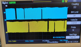
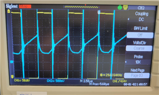
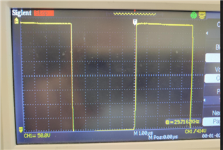
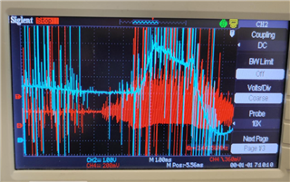
The problem I am facing is that driver outputs of UCC28070 are simultaneously switching during both half-waves. 
Usually first half wave only Q1 should switching and second half wave Q2 takes place. 
The power factor is ok, but that strange behavior makes the efficiency to drop significantly after certain power ( after 50% load ) 


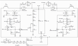
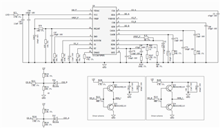
I have attached schematics and wave diagrams. 


  • Hello Ilia, 

    The UCC28070 and UCC28070A are designed for interleaved CCM boost-PFC and as such, both boost phases are intended to switch simultaneously (although interleaved by 180 degrees within a switching cycle).  When these devices are re-purposed to control the semi-bridgeless PFC, the two gate drive outputs still switch simultaneously as the device was designed to do.  This is not strange behavior; it is expected behavior. 

    During one half of the AC line cycle, one of the boost phases is active and performs PFC because the line voltage is applied to it while the other phase is inactive because only a negative diode-drop from the diode bridge is applied to it.  Switching of the MOSFET in the inactive phase has no effect except dissipate some gate-drive power.  
    When the line cycle polarity reverses, the active and inactive switching situation moves from one boost phase to the other. 

    Since this situation happens at all load levels, why do you attribute the drop in efficiency at light load to switching of the inactive phase?  
    Can you please quantify what you describe as "...efficiency...drop significantly..." and provide the test conditions for your efficiency measurements?

    Regards,
    Ulrich

  • Hello, 

    Yes I was wrong about it. 

    Efficiency is 95.5% in 300W 

    Test conditions: 

    Power transformer with watt meter -  DUT ( PFC) - Electronic load 

    PFC is designed for 700W 

    When I set the electronic load to 600W the efficiency  starts to drop with time it goes down to 92.6% and transistor temperature goes above 100 degrees, so turn of the test. 
    I cant see any overvoltage switching oscillations or current saturation 
    As you can se on the attached pictures


  • Hello Ilia, 

    I don't see any OV or saturation either.  However, I do see a lot of ringing on the current waveform especially at the turn-on transitions. 
    That, coupled with the rising transistor temperature, leads me to believe that the power dissipation in the MOSFETs is higher than expected, possibly due to two things: 
    a)  increasing reverse-recovery current from the boost diodes as their temperature rises at higher loads, and/or (probably and)
    b) High turn-on switching loss from Coss and snubber capacitances. 

    The IPB60R055CFD7 MOSFET data sheet says it is optimized for soft-switching applications and I think it may not be suitable for this hard-switched PFC application. 
    Diagram 15 in the datasheet indicates about 9uJ of energy loss (at 400V) each switching cycle, which becomes 0.9W Coss loss during the half-line-cycle in which it is active.  But the 100pF Vds snubber and 100pF diode snubber caps add their own contributions.  I make a rough guestimate of (3 x 0.9)/2 = ~1.4W from switching.  The higher load means higher conduction losses also add in. 

    A similar IBP60R060P7 device shows 7uJ energy loss/cycle at nearly the same Rds(on).  I suggest for you to find a P7 device with higher Rds(on) to reduce the Coss loss component.  The lower Coss may compensate for the higher R.

    Also, as a test, please remove the snubbers on both the Fets and the diodes and see if the device temperatures (and efficiency) improve.  

    Once acceptable stable temperatures and overall operation is achieved, then the smallest snubber networks necessary for EMI reduction can be introduced. 
    Avoid oversizing the snubbers. 

    If the above doesn't improve things, then maybe you need better heatsinking of the FETs to keep their Tj under control.  

    Regards,
    Ulrich

  • Hi Ulrich, 

    I will try those things and come back with results

  • I removed snubber, but no difference at all. Neither efficiency improved neither current oscillation improved. 
    turn on and turn off time is around 50 ns.  
    I have ordered IBP60R060P7, that will be next test. 


  • Hi Ilia, 

    When you mentioned no difference in current oscillation, I looked at the current waveform again and noticed something that I missed before.
    The signal is riding on a 500-mV pedestal.  Where is this signal being probed, please?   
    Per the schematic, R110 and R112 should apply only about 150-mV offset.  
    The high ringing on the current waveform may be coming from two sources:
    a) high inter-winding capacitance in the boost inductor ringing with that inductance, and/or
    b) the junction capacitance of the schottky diode D14, D15 ringing with the CT magnetizing inductance. 
    I think this is a side issue not involved with efficiency or MOSFET heating, but I suggest to replace the SK220A schottky with an ultrafast-recovery P-N diode.
    The peak current is low, so it can be a ~200mA size.

    If your boost inductor is constructed with overlapping turns and layers, I suggest to try a bank-winding construction which reduces winding capacitance significantly.

    I hope that the new MOSFETs will make some improvement, but also please check your heatsinking effectiveness.

    Regards,
    Ulrich

  • Hello,

    The signal is riding on a 500-mV pedestal.  Where is this signal being probed, please?   
    Per the schematic, R110 and R112 should apply only about 150-mV offset.     
    - yes below 300W the offset is 150mV , that in higher load something happens

     I have attached picture blue signal is Vsense and red is Current sense 
    after 400W regulator goes crazy. 

    After changing D14 and D15 things improved Vsense is stable but oscillation in current waveform still occurs. The efficiency improved a little bit but not what it should be.  I will consider better FAN. 

    Question is: Do you think current sense is causing unstable regulation and from there efficiency drop.
    I will try reset network with zener  and diode as shown in the datasheet and see if that will make any change. 

  • Hello Ilia, 

    The blue VSENSE signal shown in the waveform above does indeed look crazy.  I am glad that changing D14 and D15 restored stability. 

    To your question: I think the oscillations in the current waveform might still cause unstable regulation if the oscillation peaks are detected at CSA and CSB and the internal current synthesis generates the wrong down slope based on the wrong current peak. The current amplifier outputs adjust PWM to make the inductor current follow the IMO reference wave-shape.  But if the cycle by cycle signal at CSx is distorted, then the PWM will change to either pump out too much current or not enough current and this can effect the output voltage.  Then VAO voltage will try to change to regain regulation but it moves very slowly, so PFC Vout could change quite a bit while the VAO is trying to keep up with the changes. 

    There is a lot of switching noise on the VSENSE signal.  This is probably due to noise coupling to the oscilloscope probe Ground wire. 
    I recommend to use "tip & barrel" probing method to minimize switching noise pickup.   
    See this App-Note which includes a discussion on probing at pages 4-5: https://www.ti.com/lit/pdf/slua850

    You can use this method on the current sense waveform, too, at CSA and CSB to see what these signals really look like.

    I don't know what can cause the 150mV offset from R110 to suddenly increase to 500mV for load power > 300W.  I assume that the 12V source on R110 does not suddenly increase.  My guess is that the magnetizing inductance of the current-sense transformer (CT) does not get fully demagnetized and residual current is forced to flow through R112 generating the higher offset.  The zener-diode reset network might improve this situation as long as the zener has a high voltage and the diodes are rated for this high negative voltage.  

    Regards,
    Ulrich