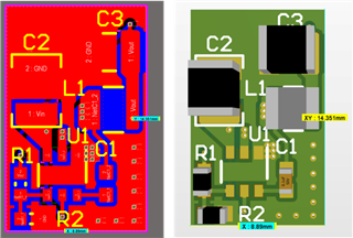
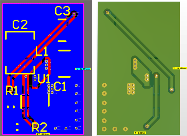
I plan to use TPS561201 to input 5V and output 2.5V, but the usable area on the PCB is only about 9mm * 19mm, so I can't design a pattern with as much margin as the evaluation board (TPS561201EVM-896).
Please provide a better way to design with this area.
The conditions are as follows:
・5V input, 2.5V output
・Current ≤0.6A
・Assumed number of board layers: 2 or 4 layers
The selected parts are:
(I selected the parts myself after looking at the recommended parameter ranges for the parts in Power Designer)
・Cin: GRM32ER71E226KE15L (22uF ±10% 25V X7R 3225 metric)
・Cbst: C0603C104K5RAC7867 (0.1uF ±10% 50V X7R 1608 metric)
・L1: DFE322512F-3R3M=P2 (3.3uH 2A 108mΩ 3225 metric)
・Rfbt: RC0603FR-0722K6L (22.6kΩ ±1% 1/10W 1608 metric)
・Rfbb: RC0603FR-0710KL (10kΩ ±1% 1/10W 1608 metric)
・Cout: GRM32ER71A476KE15L (47uF ±10% 10V X7R 3225 metric)
Best regards,
Kazuya Iwase


