This thread has been locked.

If you have a related question, please click the "Ask a related question" button in the top right corner. The newly created question will be automatically linked to this question.

BQ76942: 8 cell battery voltage monitor

Part Number: BQ76942
Other Parts Discussed in Thread: TPS3808, ISO1641, TPL5110

Hello,

I'm working on schematic for 8 cell battery voltage monitor, based on BQ7694202. Since all other features are not needed, they are disabled in a way that unused pins are connected to Vss or left floating as proposed in the table 16-3 in a datasheet.
I just would like ask for a schematic check. Schematic is available here: https://we.tl/t-2V8v50NjM8
I'm not sure if I implemented wake-up circuit in a proper way. Idea is to change BQ7694202 state from SHUTDOWN to NORMAL approx. 2 seconds (with TPS3808 IC) after battery balancer connector is connected to CN20 connector. In a such way pin TS2 is pulled down indefinitely, but I'm not sure if this is acceptable or should be pin released after some time (after device state switched to NORMAL state)? On the other side, state change from NORMAL to shutdown is guaranted when battery balancer is removed from CN20 connector. Is resistor R41 necessary or could be omitted since internal pull-up resistor is integrated in IC on TS2 pin?
What do you think about balancer resistor and balancer capacitor values (100R and 1u) since they are on the max. proposed side? Do you suggest to use lower values?
Somewhere I read that BAT and CP1 pins could be connected together if DSG and CHG pins are not used. Is this right?
Is resistor R26 needed between PACK pin and top battery cell?

Any other suggestions are welcome!

Many thanks,
Kind regards,
Dejan.

  • Hi Dejan,

    I am not able to access your schematic. You should be able to save the schematic as a PDF and attach it directly in a message on this thread.

    Regards,

    Max Verboncoeur

  • Hello Maxwell,

    thanks for your reply.
    Please find schematic here: 7853.BQ7694202_batt_monitor_sch.pdf

    Many thanks,
    Kind regards,
    Dejan.

  • Hello,

    I'm thinking about the another idea of waking up the BQ7694202 from SHUTDOWN state to NORMAL state. New idea is to leave TS2 pin floating (TPS3808 and belonging components are not needed any more in this example) and connect LD pin directly (or via 10k resistor) with the top cell of the battery and this will happen imediatelly (could be this a problem?) after connection battery balancer connector in CN20 connector. In this case a voltage on LD pin will be over wakeup threshold voltage for sure. On the other side, device will go from NORMAL to SHUTDOWN state imediatelly when battery balancer connector would be disconnected from CN20.
    In such case also additional 3V3 LDO (TPS7B6933) would not be needed, because in BQ7694202 integrated LDO could be used for powering ISO1641 I2C isolator.
    What do you think?

    Many thanks,
    Kind regards,
    Dejan.

  • Hi Dejan,

    Everything looks good, and I think both of your ideas to wake the device would work.

    I recommend releasing TS2 after the part has transitioned to NORMAL mode since leaving the pin pulled down risks the part entering a soft-shutdown state if the device ever attempts to enter shutdown mode. This soft-shutdown state is discussed at the end of Section 7.5 of the TRM.

    The 10k on TS2 should be fine, just make sure your MOSFET is low leakage.

    Regards,

    Max Verboncoeur

  • Hello Max,

    many thanks for your reply and recommendation - honestly I didn't know for soft-shutdown state before.
    It looks that one-shot generator or something like this would be necessary. I'm thinking about TPL5110 timer also.
    Questions that arise here are:
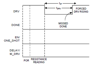
    - how long is necessary to wait between voltage on BAT pin of BQ7694202 rise to valid range and time when WAKE "pulse" is provided to TS2 pin? I'm asking this because TPL5110 timer has fixed time (POR+RESISTANCE READING) after supply voltage is provided and pulse is generated on its output. This time equals around 100 ms. I'm worry that this could be too early and would be better to wait longer that BQ7694202 IC boots up properly?
    - what is the needed length on pulse that device will change state from SHUTDOWN to NORMAL for sure? I'm thinking about 150 ms, however it looks like that change state triggers on signal falling-edge event, so even 10 ms should be enough?
    - what do you think about directly connecting TS2 pin via 10k resistor to output (DRV pin) of TSL5110? At power-on, DRV pin of TSL5110 would be on logic HIGH (3V3), after POR+RESISTANCE READING time (around 100 ms) would go to logic LOW (0V) for tDRV time (150 ms) and after that back to logic HIGH.

    TSL5110 functional mode (POT+RESISTANCE time is fixed, tDRV time is configured):

    Updated schematic: BQ7694202_batt_monitor_sch_ver2.pdf

    Many thanks,
    Kind regards,
    Dejan.

  • Hi Dejan,

    When a battery voltage is first applied, the part will automatically WAKE.

    If the SHUTDOWN function is being used, we recommend using a MOSFET to pull down the TS2 pin for wake up, and to not connect TS2 directly to the wake circuit.

    Regards,

    Max Verboncoeur

  • Hello Max,

    so every time when battery voltage is applied to BQ7694202, a device will automatically WAKE (goes to NORMAL mode)?
    If that is right, I don't need anything on TS2 pin at all, because everything I need is that when battery balancer connector is connected to CN20 connector, BQ7694202 goes from shutdown mode to normal mode and stays in this mode until balancer connector is disconnected. There will be no change in modes during device is powered-on.

    Many thanks,
    Kind regards,
    Dejan.

  • Hi Dejan,

    That is correct, when the battery voltage is first applied to the device, it will automatically WAKE, however it will typically WAKE into SLEEP mode if allowed by the device. If you only want the device to be in NORMAL mode when powered, then you can disable SLEEP and SHUTDOWN mode in the register settings and leave TS2 floating.

    Regards,

    Max Verboncoeur

  • Hi Max,

    since registers can not be changed in a SLEEP mode, I'm planning to put between TS2 and GND a switch with 10k resistor in series. So, for a very first power-on, a switch will be used to put device to a NORMAL mode. Then registers will be changed in a way that SLEEP and SHUTDOWN mode will be disabled, after that every power-on cycle, device should boot up in NORMAL mode without any switch press. Sounds this possible/correct or did I miss understand something?

    Many thanks, Dejan.

  • Hi Dejan,

    The switch will work as you've described. One thing to note is that every power cycle, the device will load it's OTP into the registers, so any changes made to just the register settings and not the OTP will not persist between power cycles.

    You can find instructions on programming the OTP in the BQ769x2 Calibration and OTP Programming Guide.

    Do keep in mind that the OTP can only be changed a limited number of times (the guide discusses the limitations in more detail), so make sure that the settings work before you write them to the OTP.

    Regards,

    Max Verboncoeur

  • Hello Max,

    can you please check schematic again, because I decided to use internal LDO and two termistors, so I added some components:BQ7694202_batt_monitor_sch_ver3.pdf

    Additional question - I'm using ALERT pin as digital output pin. Can DCHG and DDSG pins be used in the same way as digital output pins without capacitor between CP1 and BAT pin? - I omited this capacitor because DDSG and DCHG functionality will not be used.
    Is any special requirement for diode D7 and D8 or can be schottky diode used as in my example? Maximum current that would be needed from REG1 is around 15 mA or less.

    Many thanks,
    Kind regards,
    Dejan.

  • Hi Dejan,

    This all looks good to me.

    The DDSG and DCHG pins are driven by either REG18 or REG1 (depending on your settings), so there is no need for the capacitor on CP1 to use them.

    You can use a Schottky for D7 and D8. The example schematic in Section 12.2.5 of the datasheet uses Schottky diodes.

    REG1 can output up to 45mA, so there's no issue there.

    Regards,

    Max Verboncoeur

  • Hello Max,

    many thanks.
    Additionaly...do you recommend that I put a diode in series also with resistor R26 (connected to the PACK pin of BQ) shown on schematic in my previous post or diode in this example is not needed?
    Since REG2 will not be used, I'm going to leave pin "floating", so I'm planning to remove component C47 from schematic. The same example is shown in BQ's datasheet, so I think that removing REG2 capacitor must not be a problem?

    Many thanks,
    Kind regards,
    Dejan.