Hi Folks,
I have a question related to the footprint that actually have in my design for the TPS7A1650QDGNRQ1.
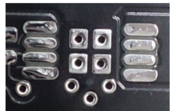
In the footprint the central pad for dissipated the heat is like a hatched (see the picture)

In the datasheet recommends a different shape pad, is a complete square pad and not hatch.

I'm Afraid that the pad has not a good o sufficient contact with the expose pad in the chip, and the thermal resistance increase.
What is the recommendation for the dissipation pad hatch or complete?
We are having thermal issues with this component; do you think is related to shape pad.
And the solder paste layer is the same hatched.
Thanks for the help.