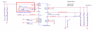
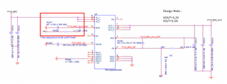
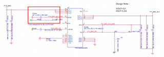
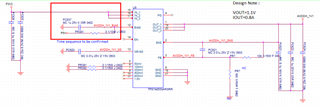
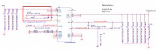
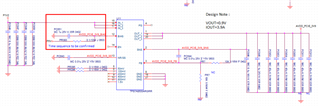
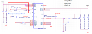
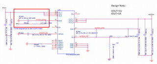
This thread has been locked.

If you have a related question, please click the "Ask a related question" button in the top right corner. The newly created question will be automatically linked to this question.

TPS7A85: Please help to check the schematic design of TPS7A8500ARGRR.

Part Number: TPS7A85

Hi TI Folks,

My case uses TPS7A8500ARGRR, please help to check the schematic design. (The voltage and current are written in the design note)

Especially Vdrop and thermal evaluation.(Vn VS Vout)

On the other hand, May I ask VBIAS under what circumstances should I pull high? Is a pull high resistor needed?

  • Hello Kuo, 

    Ensure TJ does not exceed 125C during normal operation. 

    - There is concern with current LDO selection and thermal performance. see below. 

    If using the any out connections, ensure FB resistor network stays disconnected. 

    We have sometimes seen issues with a bias ail with a pull up resistor and internal resistances interacting. If the configuration works for your application, you can continue to use it. Pull up resistor for VBIAS is not necessary, unless you're trying to make an RC filter. 

    Important comments for all schematics:

    - There is no net tied to EN. 

    - If you want to use the PG signal, a pull-up resistor must be connected to the pin. 

    - A 10uF capacitor must be connected to VBIAS if the rail is being used. 

    - A 47uF capacitor - 25minimum capacitance- must be connected to the output of the LDO

    U5

    PD = (3.3-2.5)(0.5)W = 0.4W

    TJ = TA + (0.4)(35.4)C = TA + 14.16C


    U6

    PD = (1.8-1.2)(1.5)W = 0.9W

    TJ = TA + (0.9)(35.4)C = TA + 31.86C


    U7

    PD = (1.8-1)(1.5)W = 1.2W

    TJ = TA + (1.2)(35.4)C = TA + 42.48C


    U9

    PD = (3.3-1.1)(.8)W = 1.76W

    TJ = TA + (1.76)(35.4)C = TA + 62.304C


    U10

    Current Voltage set to 0.95V

    PD = (1.2-0.95)(3)W = 0.75W

    TJ = TA + (0.75)(35.4)C = TA + 26.55C


    U11

    Current Voltage set to 0.95V

    PD = (1.2-0.95)(3.9)W = 0.975W

    TJ = TA + (0.975)(35.4)C = TA + 34.515C


    U15

    PD = (3.3-1)(1)W = 2.3W

    TJ = TA + (2.3)(35.4)C = TA + 81.42C


    U16

    PD = (3.3-1)(1)W = 0.975W

    TJ = TA + (0.975)(35.4)C = TA + 81.42C

    Best,

    Juliette

  • Hi Jullette

    So my Vin/Vout is ok and no LDO drop out issue?

    Thank you.

  • There are concerns over the power dissipation of some devices. What is the ambient temperature of your application?

    Best,

    Juliette

  • Hi Juliette,

    The TA is 45C.

    Thank you.

  • Hello Kuo,

    At that ambient temperature, U16 and U15 risk going into thermal shutdown. Extra care must be taken when laying out these devices, and a heatsink may be necessary. 

    Please refer to this: An empirical analysis of the impact of board layout on LDO thermal performance

    Best,

    Juliette