This thread has been locked.

If you have a related question, please click the "Ask a related question" button in the top right corner. The newly created question will be automatically linked to this question.

UCC27282: Built-in bootstrap diode

Part Number: UCC27282

Hi All,

I have a question regarding UCC27282.

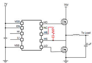
How much current can be continuously passed through the built-in bootstrap diode?
Also, what is the maximum value of pulse current? For example, I would like to check how much current can flow when initially charging the bootstrap capacitor.

The maximum value of HB quiescent current (IHB) in 6.5 Electrical Characteristics is 0.4mA.


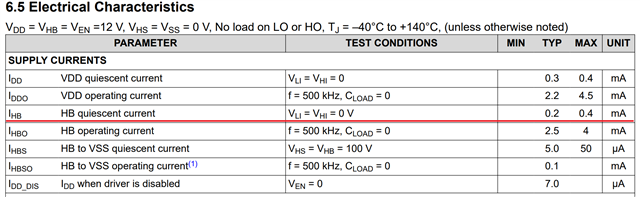
Figure 6-2. HB Quiescent Current is 0.18mA at maximum.


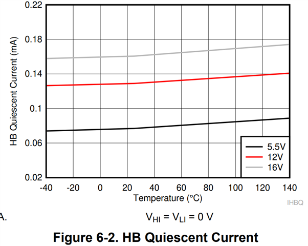
What's the difference? Is the maximum 0.4mA due to device variations? Or are there other conditions?

Best Regards,
Ishiwata

  • Hey Ishiwata,

    Thank you for your question regarding the UCC27282.

    For the bootstrap diode current maximums, the diode average current should be kept below 80mA. This average value can be found by using the switching frequency (Fsw) and the total charge Qg of the high side FET that is connected to the HO pin (I = Qg * Fsw). This device does not have an internal series resistance with the bootstrap diode but the diode's dynamic impedance (approximately 1.5 Ohms) helps to limit the peak forward current and prevents damage in most applications. In high switching frequency (Fsw>1MHz) applications where a small low-side minimum pulse width is used, the peak diode forward and reverse current would be very high and so we would recommend an external Schottky bootstrap diode.

    For the maximum HB quiescent current, this maximum and typical value is done under the same testing conditions other than temperature. So this would be due to device variations and response to different temperatures.

    Let me know if there are any further questions.

    Thank you,

    William Moore

  • Hi William,


    Thank you for your reply. It's a big help.

    I may not understand it correctly, but
    what is the maximum value of pulse current? For example, I would like to check how much current can flow when initially charging the bootstrap capacitor.

    I have an additional question.
    Insert a resistor between the HB and HS terminals as shown below to limit the current to the bootstrap capacitor. Will such a circuit affect the operation of the IC?

    Thank you for your support.


    Best Regards,
    Ishiwata

  • Hey Ishiwata,

    There is not a specified value as to maximum pulse current because there are many factors to take into consideration such as slew rate, dead time, and pulse duration. But, you can control how much current can flow during start up with a bootstrap resistor. Further information on how you select this resistor and how it affects the circuit can be found in the Bootstrap Circuitry Selection for Half Bridge Configurations App Note in Section 3.4. Your idea to put this resistor in series is correct, but typically that resistor should be placed in series at the VDD pin. This bootstrap resistor will limit the peak current on the diode during start up.

    Let me know if you have any further questions.

    Thank you,

    William Moore

  • Hi William,

    Thank you for your reply.

    Regarding the resistor and capacitor between the HB and HS terminals, is the circuit you recommend below correct?Limit the peak current with a resistor when input to VDD?

    Best Regards,
    Ishiwata

  • Hi Ishiwata-san,

    Both options (resistor on VDD and resistor on HB) are viable. If you trace the turn on loops, you can see that this resistor does have some consequences. The resistor on VDD is in series with the:

    1. LO turn on loop (so it acts like gate resistor, and has a voltage drop)
    2. Bootstrap diode (so it limits that current like you wanted)

    The resistor on HB does the same thing but only to the HO turn on instead of LO.

    Another option is to place a resistor between HS of the device and the drain of the low-side FET. That also has drawbacks:

    1. The voltage drop across that resistor creates a Vgs on the high-side FET
    2. It is in the turn-off loop of the high side.

    Sorry for the long answer, but there are trade-offs to all of these options. 

    Thanks,

    Alex M.

  • Hi William,


    Thank you for your reply. It's a big help.

    I would like to confirm whether my understanding is correct.
    In the case of the circuit below, it is possible to limit the current, but the disadvantage is that HO acts like a gate resistor, so a voltage drop will occur, so care must be taken.
    Is my understanding correct?

    Thank you for your support.


    Best Regards,
    Ishiwata

  • Hi Ishiwata-san,

    That is correct. For example, there is a UVLO circuit on HB, which may trigger if the drop is large enough. 

    Thanks,

    Alex M.