This thread has been locked.

If you have a related question, please click the "Ask a related question" button in the top right corner. The newly created question will be automatically linked to this question.

LM5161: Input side spike noise reduction method

Part Number: LM5161
Other Parts Discussed in Thread: SN6505B

Hi experts.

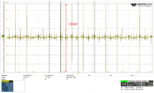
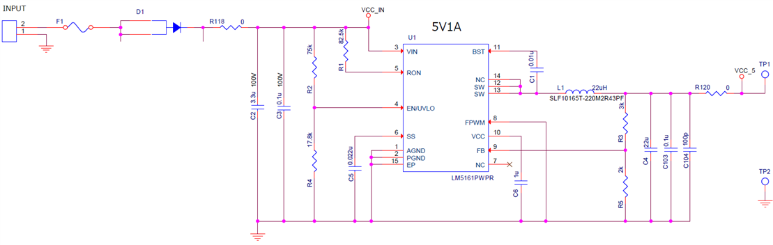
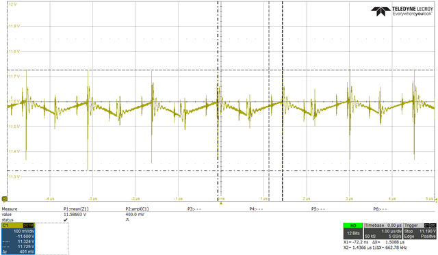
I calculated the input capacitor to be 3.3u and 0.1u using the formula in the data sheet,

but the spike noise on the input side is about 1.5V.

Installing a larger capacitor will reduce noise, but this is not practical due to space considerations.

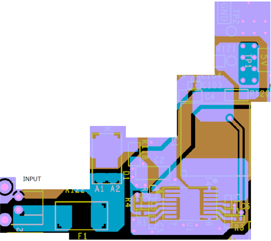
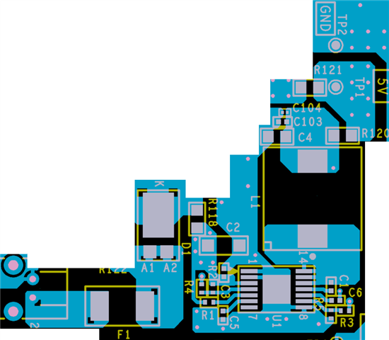
I would like to receive advice on noise countermeasures, such as input capacitor selection, component placement, and GND routing in the case of a 4-layer board.

  • Hello,

    Do you have waveforms that you can share to show what you mean by "spike noise" ?

    If you are talking about EMI, here is an application note on input EMI filters: https://www.ti.com/lit/an/snva489c/snva489c.pdf

    Please also share schematics and layout with the corresponding operating conditions.

    Best regards,

    Ridge

  • Hello.

    This is the measured waveform of 3 pins of LM5161 when using a ground spring. GND is taken from a nearby via.

    The filter described in AN-2162 is certainly effective, but requires large capacitors and takes up a lot of space.

    I also share the schematic and layout.

  • Hello, 

    I am actively looking into this issue. In the meantime, can you confirm the input voltage range for your design?

    Some general comments for now:

    • Make sure that the input capacitors are placed as close to the input of the IC as possible on the PCB
    • C2 looks far from the IC in the screenshot you shared
    • NC pins should have no connection. It looks like one of the NC pins is connected to the SW node

    I have one last question for the PCB: I see the different purple, blue and brown layers, how is the Vin pin connected to the rest of the Vin path?

    It does not look like there is a via or component connected to the purple node for D1 and R118 to the input pin of the IC.

    Best regards,

    Ridge

  • Hello


    Thank you for your reply.

    The input voltage range is 8-52V.

    Pin 14 is connected in the evaluation board circuit, but is it better not to connect it?

    D1→R118→Vin pins are connected on the component side. The via near R118 is connected to the inner power layer.

    The layout shown last time is difficult to understand, so I will show only the layout of the component side.

    Best regards

  • Hello,

    Thank you for sharing the new image of the layout. For the layout, the GND pins should be connected with direct pours rather than the thin connections as shown. The return path to the IC, as shown, is longer than it needs to be which can increase inductance in the return loop, which could hurt EMI performance. If your schematic follows the EVM for the NC pin, it will be OK. The SW node pins could also be connected with direct pours.

    Looking at the layout and the waveform, there are a lot of spikes that seem out of place. I have the following questions:

    • Are there multiple switching power supplies connected to the voltage rail? The extra spikes make it seem like that is possible
    • What bandwidth are you measuring or trying to filter? At some point, the input filter will be necessary 
    • Can you share a photo of the lab setup and is it possible for you to measure directly over the C3 capacitor? It could be that some noise is getting coupled into your measurement from the position of the scope probe. A photo of the setup would help rule this out.

    Best regards,

    Ridge

  • Hello,

    Thank you. I understood to connect the GND pin directly.

    As for the other switching power supply, the SN6505B is connected to the output of the LM5161.

    This board mostly operates under light loads, and noise of around 20kHz was observed in DCM mode, so I would like to filter out noise around this area.

    I will share the waveforms measured at both ends of C3 using a ground spring.

    I'm sorry, but it's difficult to take pictures, so I'll show you the configuration when I measured it.

    Best regards.

  • Hello,

    The latest waveform looks more reasonable. However, you could add another high frequency capacitor in parallel with the one you already have. Increasing the input capacitance will also help. It is possible that there is too much ESR that is causing some of the noise. 

    If you are concerned with noise affecting the input line of your board, then you will need an input EMI filter. I have copied the link to the previously mentioned app note here: https://www.ti.com/lit/an/snva489c/snva489c.pdf

    Best regards,

    Ridge 

  • Hello,

    Thank you teaching me.

    I found out that what I can do is:
    ・Connect the input capacitor directly near the IC.
    ・Add input capacitor.

    Best regards.

  • Hello,

    Glad we could help. For now, I am going to close this thread. If you have more questions, you can re-open this thread by replying or you can open a brand-new thread.

    Best regards,

    Ridge