This thread has been locked.

If you have a related question, please click the "Ask a related question" button in the top right corner. The newly created question will be automatically linked to this question.

TPS272C45: Parasitic capacitance @output

Part Number: TPS272C45

Hello,

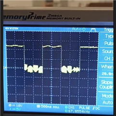
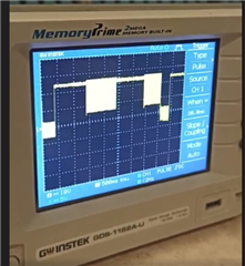
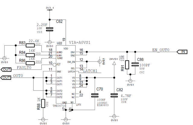
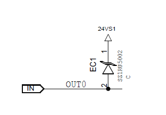
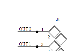
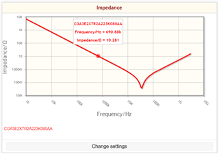
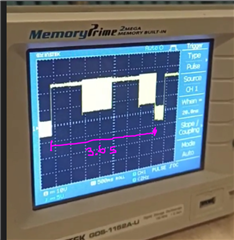
With IEC 61000 4-6 test (conducted disturbance 10V, up to 20V, frequency between 400kHz -900kHz) output that is in the OFF state charges to some potential all the way to power supply voltage.
In this case it charges to 24V. We do not have output capacitor.
Only these frequencies are problematic. Other ones are without issues.

It is maybe related to previous post where Output self charge even when there is no capacitance at output.

Best regards,
Miroslav

  • Hi Miroslav, 

    Could you describe your exact concern? Perhaps you can link to the previous post you are referring to; I am not sure what your question is here. 

    At what frequencies are you observing problematic issues, and what is the issue? Waveform captures and a schematic would also be helpful. 

    Thank you! 

    Best Regards, 

    Elizabeth 

  • Hello Elizabeth,

    I think that relation is some internal parasitic capacitance. Maye they are related, maybe not. But clearly something behaves very strange.
    Here are 2 pictures of Outputs, one is with MOSFET discrete solution and the other one is with TPS272C45. Both are without capacitance at the output.
    We are switching output at 1s ON/OFF, and critical frequency is around 720kHz.

    As you can see, on a MOSFET solution we have some disturbance but still able to distinguish between ON and OFF.

    But with HS switch in some cases output seems not turning OFF at all, like noise accumulate in some capacitance.

    What could be the cause of this?

    Thanx,
    Miroslav

  • Hi Miroslav, 

    A schematic along with a waveform depicting VS and EN along with Vout would be needed to determine root cause of this. 

    Is this happening at all frequencies  400kHz -900kHz, or just some frequencies in that range? 

    Best Regards, 

    Elizabeth

  • Hello Elizabeth,

    We have only TVS diode @output, critical frequency is around 700kHz. I is done during test when frequencies are changing all the time so we could not fix it on a single one. 

    Best regards,
    Miroslav

  • Hi Miroslav, 

    It sounds like you are preforming some sort of EMI testing? 

    If so, I would recommend using the recommended external components listed in Table 10-1 of the datasheet, specifically the output capacitor of 22nF I am not seeing in your schematic. 

    Best Regards, 

    Elizabeth 

  • Hello Elizabeth,

    We do have 22nF as well on new design. But situation is even worse, because problematic frequencies starts at already 500kHz.(without 22nF starts at 700kHz)
    To relate this to previous topic, without external capacitor output charges up to some voltage and when you touch it with wire to ground -> it sparks!?!?!?!
    To get it to spark state we need to wait some time, maybe one minute.  Output charges even faster with external capacitor but it is more less easy to understand. But without...it is not normal.

    We do not have a problem with sparking, it is unimportant for us. But this EMI is a problem. Please explore this topic further.

    Best regards,
    Miroslav

  • Hi Miroslav, 

    That is interesting. I am reaching out internally to see if we have any recommendations for external circuitry with IEC 61000 in mind.

    Is there a particular reason this standard is required for your application? 

    Any further clarification would be helpful in ensure we can provide the best solution for your application. 

    Best Regards, 

    Elizabeth

  • Hello Elizabeth,

    61000-4-6 and 4-16 are both making troubles. They are based on similar disturbance approach.
    They are both required for our product :( 

    Worth mentioning is that we have load of 2mA during the test on output and this is not enough to eliminate disturbance.
    50mA load is eliminating it. Maybe even less but we didn't tested. Load is not a capacitive but resistive.

    Best regards,
    Miroslav

  • Hi Miroslav, 

    Unfortunately, the only IEC 61000 result I have is for IEC 61000 4-5, which we pass. 

    If you can provide more details on the 4-6 and 4-16 standard, perhaps we can see what effort is needed to pass those standards. 

    Best Regards, 

    Elizabeth 

  • Hello Elizabeth,

    Maybe you can find out more from this link https://www.atecorp.com/compliance-standards/iec/iec-61000-4-6 

    Or this one https://www.emcstandards.co.uk/files/61000-4-6_immunity_to_conducted_rfi_2_1.pdf 

    Those ones I was able to search on internet that are accessible. Thanx to authors

    Best regards,
    Miroslav

  • Hi Miroslav, 

    Thank you for sending those resources. We are reviewing them internally to see what solutions we can offer. 

    I will update you later today. 

    Best Regards, 

    Elizabeth 

  • Hi Miroslav, 

    To confirm, you've mentioned the 22nF output capacitor we recommend as an external component was causing the problematic frequencies to start at 500kHz rather than at 700kHz without the recommended output capacitor; is this correct? 

    We would expect the 22nF to absorb the RF disturbance or at the lease improve the results. Would you please share the relevant layout files so we can see where the output capacitor was placed? 

    Could you also provide the part number for the 22nF so we can check the voltage rating and specifications? 

    Thank you!

    Best Regards, 

    Elizabeth 

  • Hello,

    That is true, without cap it starts at 700kHz.

    But the point is...it starts anyhow. Better question for this would be what is the purpose of this capacitor. Clearly it is not for this kind of noise so lets remove it from discussion. I'm really sure it is related to some leakage currents.
    My suggestion is to focus on maybe charge pump during negative noise, or anything that could bring voltage at higher value than ground and keep it stable (please check initial pictures).
    Here is part number C0603C223K1RACTU

    Best regards,
    Miroslav

  • Hi Miroslav, 

    The reason a capacitor near the connector would help is a capacitor functions as a shunt to ground at high frequency. If we take a look at the capacitor on our evaluation module (C0603C223K1RAC7867), the device has an impendence of ~10ohms at 700MHz.

    I am unfortunately not seeing a similar plot for the capacitor part number you have provided, but it should be a similar curve. To further this example, using the EVM capacitor on the output at 700MHz, if the capacitor is soldered down and placed next to the connector, the disturbance will go to ground through 10ohms. 

    Loading the device (for example when you are drawing 50mA) would solve this issue in a similar way. A load provides a path for the disturbance to go to ground, reducing the power the device sees at the output. 

    Without any external circuitry, a 20V conducted disturbance at the output could bias the gate if it is stronger than the pull-down structure on the gate and the device's digital protection. In this case, the device could hold up the output high as you are seeing. What we need to do is mitigate this voltage. 

    Some questions for you which would be very helpful for our debug:

    • After reviewing the standard you provided, it appears the voltage for the test should be at most 10V under a level 3/Zone C condition; is there a particular reason 20V is being attempted here? Is 20V adherence required for the end-product?
    • Interestingly, it appears the device does recover after ~3.6 seconds and goes low as shown below. Is this 3.6s the duration of the conducted disturbance, or is the disturbance still present after the time highlighted in pink below: 
    • Can you probe VDD at this time? A high VDD would be important to ensuring the digital protections are in place. 
    • Without the 22nF capacitor, my understanding is the device failed from 700kHz-900kHz; were higher frequencies >900kHz attempted, and did they pass? 

    Thank you! 

    -Elizabeth 

  • Hello Elizabeth,

    Higher frequencies, above 900kHz are completed without issues. I agree for the capacitor and high frequencies but we are very low compared to those.

    As you can see from the picture, output is not "ON" but something in between. As far I understand, this is sine wave with this 10V, 15 or 20 amplitude. So I suppose it could be one of the reason.
    But I think that true reason could be "frequency sweep", example: after 3.6s, frequency has been changed and output reacts different to that one. I think this picture is from the end of sweep range 400-900kHz and after this final one there are no disturbance anymore.

    Regarding 20V...it cant pass even 10V so no need to answer that for now I think.

    We plan to test it tomorrow with clamp diode towards ground instead of 24V.

    Thanx,
    Miroslav

  • Hi Miroslav, 

    Thank you for providing that information! 

    We suspect the reason the device is not turning fully off is gate to source coupling through the internal gate to source capacitor causing the gate to charge. 

    To reduce the power seen at the output and allow the gate to pull low, we need to diffuse the disturbance to ground. This can be done using a capacitor soldered down and placed close to the connector. 

    I suspect the issue with the current setup is the capacitor being used, and where it's placed. If a 50mA load (400ohm load) resolves the disturbance, then a capacitor which is 10ohms at 400-900kHz should resolve the disturbance similarly. 

    I am not able to find any frequency vs. impedance information on the capacitor you are using; would it be possible to use a C0603C223K1RAC7867 capacitor soldered down and as close to the external connector as possible and rerun the test? 

    Best Regards, 

    Elizabeth 

  • Hi Miroslav, 

    Reaching out to see if any further results have been collected. 

    Happy to hop on a call to further discuss if needed. 

    Best Regards, 

    Elizabeth 

  • Hello Elizabeth,

    Thanx for support. Due to lab limitations, tomorrow we will have an update for you.
    But it is totally related to output capacitor

    Best regards,
    Miroslav

  • Hi Miroslav, 

    Were you able to solve this issue? 

    Happy to provide support if needed. 

    Best Regards, 

    Elizabeth 

  • Hello Elizabeth,

    It was due to capacitor value or quality. 
    So increasing capacitor value solved the problem. Thank you for support.

    I would have a very last question for you, would capacitor increase to ~100nF from 22nF potentially affect any other standard or test?

    Best regards,
    Miroslav

  • Hi Miroslav, 

    Happy to hear increasing the capacitor value resolved the issue. 

    It is possible the increased capacitance could affect other standards or tests as they are very system dependent. 

    For clarification on our 22nF recommendation, we recommend an output capacitance of 22nF for the purpose of filtering out voltage transients (for example, ESD, RF transients), and additional capacitance to that will help filter out voltage transients with eventually diminishing returns. 

    While I do not foresee a concern, our recommendation is to test all of the standards you need to pass to ensure your solution is robust. 

    Best Regards, 

    Elizabeth