This thread has been locked.

If you have a related question, please click the "Ask a related question" button in the top right corner. The newly created question will be automatically linked to this question.

TPS40200 adjust gate drive voltage?


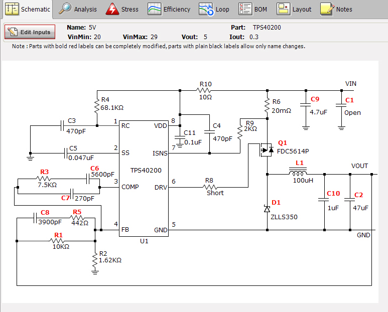
What is the best way to adjust the gate drive voltage for the TPS40200-- normally, Vgs is -8V, for the mosfet I'm using I need this to be -5V at the most (lowest).  

I'm stuck with that particular mosfet.


Thanks!

Andy


  • Hi Andrew,

    Could you provide more information about your design specs, like Vin, Vout, Iout, Fsw, the part number of the FET?

    Regards,

    Na

  • HI Na-

    The P-Channel Mosfet is: CHT-PMOS3002-TO254-T

    http://www.cissoid.com/images/stories/pdf/Datasheets/cht-pmos30xx.pdf

    Fsw can be whatever works-  I think it's currently a few kHz
    Vin 20-29 V
    Vout 5V, (15V for another supply)
    Iout: 300mA
    I've enclosed a picture of what I'm doing so far (from TI switcher software), for 5V
    Thanks-
    Andy

  • Hi Andy,

    In order to clampt the gate voltage not lower than VIN-5V, a zener diode with a breakdown voltage lower than 5V but higher than the threshold of the PMOS can be used. But for the internal driver circuit design, DRV will be pulled down to VIN-8 by an internal NMOS then the NMOS is shut off. Therefore, if holding the voltage between VIN to DRV to less than 8V, the NMOS will not be able to turn off, which causes short through from the supply to ground. To solve the problem, we propose to add a resistor between DRV and the gate of the PMOS and rely on this resistor to cause enough voltage drop to shut off the internal NMOS. For the worst case, the minimum pull down current is 200mA, the maximum gate driver output voltage for 12V < VDD < 52V is 10V, if assuming the zener diode clamps at 4.7V, the minimum resistor value is

    Rmin = (10-4.7)V/200mA = 26.5 ohm.

    So I choose a 4.7 zener and 30ohm resistor to replace D1 and R5 of TPS40200EVM-001. The EVM still works fine for 12V input and 3.3V output. Please refer to the attached file for the test waveforms. The gate voltage is clampt at 4.7V and the spike is about 5.3V but still below the abs maximum voltage of 6V for the specified PMOS for your design. The penalty of adding the 30ohm resistor is longer rising and falling time of the gate signal, hence more switching losses. If it is acceptable for you, you may try this solution on your design.

    If you need more help, please let me know.

    2133.TPS40200EVM_4.7Vzener.docx

    Regards,

    Na


  • Na-

    Thanks for the quick response, info, and actually testing in hardware!

    I'll give it a try-

    Andy


  • Hi Na-

    I'll looking into an alternate approach to adjust the gate drive.  The solution you proposed with a 4.7V Zener works fine however at my operating temperature (approaching 200 deg C), readily available zeners derate to 0 W.  (And ones that would potentially work are very hard to come by).

    I'm considering a simpler voltage divider approach, with a 30 ohm resistor between DRV and the gate drive on the PMOS (as you suggested with the zener), and then a second 30 ohm resistor between PMOS gate and source.  Without looking into this too deeply I expected the Vgs to be divided from -8V to -4V-- but I'm actually getting -2V which still works experimentally.  The gate pulses are not very clean though.  (I realize this wastes current, but that's ok as long as it's ~10mA)


    I would appreciate any thoughts/opinions you have on this approach, to optimize this, etc.


    Thanks!

    Andy

  • Hi Andy,

    Since this approach works, you may keep it but adjust the two resistors to reduce some losses. Lower gate voltage, higher Rds,on and more conduction loss. So you may want to increase the resistor value between gate and source and decrease the one between DRV and gate. The reason why the voltage drop on two resistors are different is the resistor between DRV and gate has more current coming from the gate capacitance discharging.

    Regards,

    Na