Hi team,
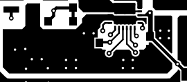
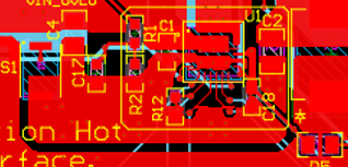
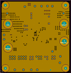
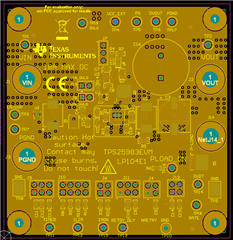
The datasheet only shows top/bottom layers of PCB image. I think there should be internal layers because I can't find routing from ILIM, ITIMER pins etc. to headers(J9, J10 etc.). Also, GND plane of the IC looks floating.


Could you please provide PCB image of internal layers?
Best regards,
Shota Mago


