This thread has been locked.

If you have a related question, please click the "Ask a related question" button in the top right corner. The newly created question will be automatically linked to this question.

UCC2818: about internal block diagram

Part Number: UCC2818
Other Parts Discussed in Thread: TPS62933

Hi,

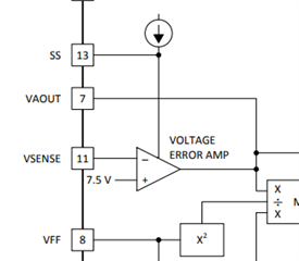
I checked the internal block diagram of UCC2818.

It looks like the input from SS pin is connected as power for ERROR AMP.

↓UCC2818

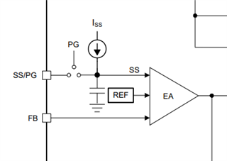
Is it correct that the connection diagram between SS pin and ERROR AMP in UCC2818 is the same as the connection diagram in TPS62933?

↓TPS62933

Best Regards,

Nishie

  • Hello Nishi, 

    Yes, you may consider the UCC2818 SS input to be connected to the Error Amplifier in the same manner as shown in the TPS62933 diagram. 

    In the UCC2818, the SS pin is NOT a power source for the EA, it is just another input that over-rides the VSENSE input during soft-start.

    Regards,

    Ulrich