A related question is a question created from another question. When the related question is created, it will be automatically linked to the original question.
If you have a related question, please click the "Ask a related question" button in the top right corner. The newly created question will be automatically linked to this question.
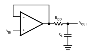
If the load capacitance is outside 0.1uF to 10uF, then we cannot guarantee stable operation of the device. I would recommend to stay within the range specified in the datasheet that you highlighted.
If the load capacitance cannot be changed, you can consider a voltage reference such as REF5030 (max load capacitance of 50uF) or REF54 (max load capacitance 100uF).
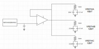
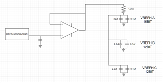
The reference chip provides power to the VREFHI of the DSP (28P65), and the DSP requires a capacitance of 22*3μF. In addition, the reference voltages for two other chips each require 10μF.
I have looked through the TMS320F28P65x Technical Reference, and section 18.14.6 has this suggested circuit for the external reference:
Are you planning on using a circuit design similar to this? If you are, then it seems that CA would be 22µF after the voltage reference for the 16-bit single ended ADC (all other ADC seem to need a 2.2 µF capacitor). They also don't seem to use an isolation resistor.
Additionally, what are the other chips that you are driving using REF3430 that require a 10 µF capacitor?
Going back to your original question about the load capacitance of REF3430, if you were to use a reference circuit like the one in the Technical Reference for the 28P65, and if you were to use the 0.1µF capacitors for DRV8316, there should be no issues using REF3430 in this application.
Here are my suggestions in response to your other queries:
Additionally, Can I use one operational amplifier to drive three ADCs for the DSP?
As is pointed out in section 18.14.6 of the technical reference guide there can be slightly decreased performance if reference pins share an op-amp driver, but in general this type of circuit does work for a generic ADC. I will invite someone who is more knowledgeable on that part to comment on whether or not using one op amp to drive the reference for all three ADCs would be acceptable.
Specific to the F28P65x application, how are you intending to use REF34xx to supply VREFHI? Could you provide a diagram so we can make suggestions? Also what is the intended ADC mode usage, is it purely 12-bit mode or would you also use 16-bit mode?
It's not recommended to operate the ADCs in different modes where one is running as 16-bit and the other two as 12-bit. This falls under the async operation where conversion noise may couple at the VREFLO lines. See ADC chapter section 18.14.1 (Ensuring Asynchronous Operation). Basic premise is that all ADCs should be triggered a the same time, and all the S/H times be the same so that conversion phase for all the 3 ADCs will happen at the same time. 12-bit and 16-bit ADC timings are different so operating one in 16-bit mode while the other 2 are in 12-bit mode would essentially put the conversion operations in asynchronous mode. Asynchronous mode of operation produces crosstalk from the conversion phase and this is enough to degrade the performance of the ADC. This will be a bigger concern the VREFHI configuration topology.
All 3 ADCs should be operated as 16-bit mode or 12-bit mode. The only exception here is that if the 16-bit mode ADC is running, then none of the 2 ADCs should be converting and the other way around.