This thread has been locked.

If you have a related question, please click the "Ask a related question" button in the top right corner. The newly created question will be automatically linked to this question.

LM5020: LM5020

Part Number: LM5020

Hi ,

We use LM5020 as flyback convert ,

Vin Max is 60V ,Output is 10.4V  1W ,Fsw :450kHZ  , CS pin resistor is 0.9ohm

Flyback has 3 output ,the voltage is both 10.4V , Voltage feed back from the Auxiliary source .

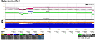
Our test condition is :Vin change from 38V to 60V ,Auxiliary output add 0.1A current ,after about 5000 times cycle test , the wave is abnormal 

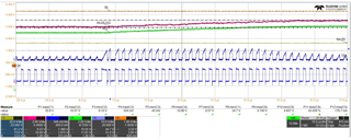
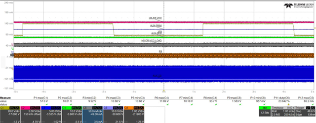
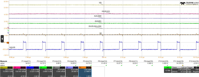
C1 :VIN   C2:Auxiliary  output  C3: CS   C6: out pin 

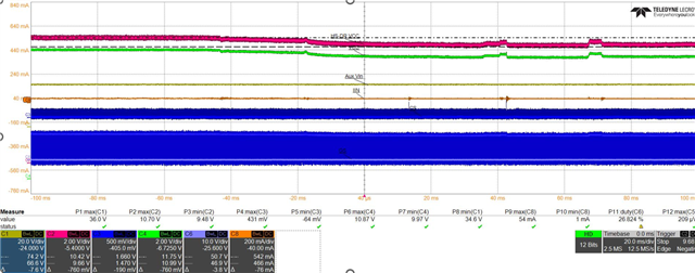
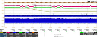
The output voltage (C2)  is unstable , it down to about 9V and then up to Normal voltage , when the output  voltage change from low to normal we can find CS pin voltage above 0.5V ,the duty increade , but the FB voltage is stable (Picture 3 ,C8)

Question : 1. Why the output unstable ?

                  2. The output is unstable ,but the FB voltage is stable ,is it right ?

                   3. CS over 0.5v ,but it doesn't like OCP ,

                   4. Duty increase  lead to  CS voltage increase , or CS increase lead to Duty increase ?

Looking forward to your reply ,thank you.
  • Hello Haixian,
    Thanks for reaching out to us via e2e.

    The feedback voltage should not remain so stable as seen in your screenshot. So, there must be something wrong.

    Would it possible for you to share a schematic with me?
    This should help me to understand how your Aux supply and feedback have been implemented.
    And also, I hope that I can then better understand some of the signal names that you are using.

    I have many other questions:
    Is it correct that the regular load is 1W?
    So, the maximum load current would be around 100mA?
    Or is this 1W load just for test purposes?

    With a current sense resistor of 900 Milliohm, you would need an inductor current of 550 Milliamps to reach the 0.5V threshold.
    At 60V input voltage this would be 33W input power, not just 1W.

    I understand that in your test you are changing the input voltage between 38V and 60V every few seconds.
    But what do you mean when you say: "Auxiliary output add 0.1A current"? Are you using a load which is constantly drawing 0.1A current?
    Or is the load current dynamically changing as well?

    When you say: "after about 5000 times cycle test, the wave is abnormal", what exactly does this mean?
    - Does 5000 times cycle test mean that the input voltage is getting switched between 38V and 60V for 5000 times before the problem occurs?
    - What exactly does "abnormal" mean? Is it the voltage drop from 10,4V to 9V?
    - Does this drop happen in the same way on all secondary voltages? (Load, Auxiliary, and is there actually a third output?)
    - Does that voltage drop occur permanently after 5000 cycles? Or sporadically every few cycles? Or is it just a single event and 5then it goes back to normal for a long time?

    And finally, I wonder why the Aux voltages are dropping BEFORE the input voltage is jumping up from 38V to 50V.
    How can this happen?

    The more detailed information I can get, the better chance we have that I can understand and help you.

    Best regards
    Harry

  • Hello Harry
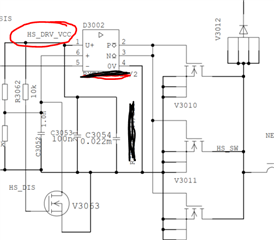
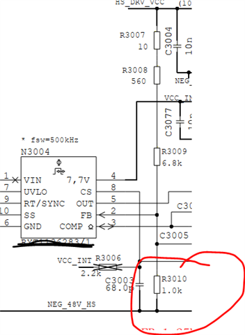
    Thanks for your confirm.                                                                                                                                                                                                                 Below is our schematic ,For your reference.About your question ,please refer my answer,thank you.

    Q1: Is it correct that the regular load is 1W?

     Answer:  The flyback circuit convert 3 output ,these output maily used for mosfet  gate driver , each output current is less than 150mA ,so the Max current of the flyback is less than 450mA 

    Q2: what do you mean when you say: "Auxiliary output add 0.1A current"? Are you using a load which is constantly drawing 0.1A current?
          Or is the load current dynamically changing as well?                                                                                                                                                                  Answer : Please refer the schematic , The input change from 60V to 38V every 3 seconds.  and we use electronic load to add  constantly 0.1A at                       HS_DR_VCC output 

    Q3: When you say: "after about 5000 times cycle test, the wave is abnormal", what exactly does this mean?
     Answer : yes ,5000 times cycle test mean that the input voltage is getting switched between 38V and 60V for 5000 times before the problem occurs 

    Q4: What exactly does "abnormal" mean? Is it the voltage drop from 10,4V to 9V?

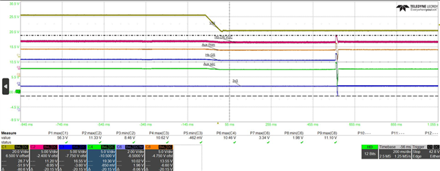
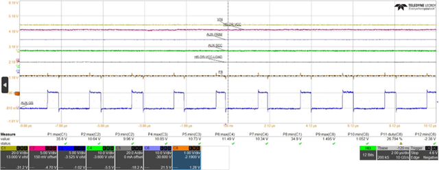
     Answer :The output of HS_DR_VCC is 10.4V ,it is ok at the begin of the test ,but after  5000 times input change  ,we catch this wave , HS_DR_VCC  unstable,it drop to about 9V and try to restore to 10.4V, and we expand the wave found ,when HS_DR_VCC change from 9V to 10.4V , CS voltage over 500mV , and the duty increase . though the output changed ,but FB voltage is stable ,so it looks like strange.

    Q5: Does this drop happen in the same way on all secondary voltages? (Load, Auxiliary, and is there actually a third output?) 

    Answer: Yes , other two voltage (AUX_SEC ,Aux_Prim ) happen in the same way ,please refer below wave

    Q6: Does that voltage drop occur permanently after 5000 cycles? Or sporadically every few cycles? Or is it just a single event and 5then it goes back to             normal for a long time?
    Answer : After 5000 cycle it is can permanently occur ,but if we power off the board for some time and then power on ,it goes  back to normal , but it can occurs again when we do the same test again ,but it need a long time to reproduce.

    Q7: And finally, I wonder why the Aux voltages are dropping BEFORE the input voltage is jumping up from 38V to 60V.
    How can this happen?

    Answer : the abnormal voltage didn't happen at the time that voltage change ,it only happen at 38V or 60V (the voltage is stable)  

    the second wave is the first time we catch the output voltage drop after long time test ,and  then we can see the output try to restoe to normal ,and CS incrase ,We also want to know why this happen Slight smile

    Hope my answer is clearly ,and forward to your reply ,

    Thank you very much.


  • Hello Haixian,
    Thanks for the explanations.

    You have stated that the three yellow marked signals are the three outputs.

    Can you please describe which signal HS_DR_VCC_LOAD is?
    (I cannot find it in the schematic)

    What is the difference between HS_DR_VCC_LOAD and HS_DR_VCC (C5 vs. C2 in the third image of your first post)?

    Is there any load connected to the HS_DRV_VCC signal?
    Which kind of load is that?
    Does it bring an own input capacitor (some additional capacitance in parallel to C3004 and C3008)?

    In other words, why is channel C5 ( HS_DR_VCC_LOAD) stable while channel C2 (HS_DR_VCC) drops?

    I assume that the names of the third oscilloscope screenshot do not actually match with the name in the schematic.
    Is the voltage that is measured at C3004 and C3008 dropping or is it stable?

    If it drops, how can the divided down version of this voltage (which is FB) be stable?

    Please clarify.

    Thanks and regards,
    Harry

  • Hello Harry
    Thanks for your confirm.

    Q1:Can you please describe which signal HS_DR_VCC_LOAD is?

    What is the difference between HS_DR_VCC_LOAD and HS_DR_VCC (C5 vs. C2 in the third image of your first post)?

    Answer : HS_DR_VCC is the voltage signal  ,HS_DR_VCC_LOAD is the current signal (we use Electronic load add 0.1A )

    this wave I want show you the FB is stable when HS_DR_VCC voltage change .

    Q2: Is there any load connected to the HS_DRV_VCC signal?
    Which kind of load is that?

    Answer:HS_DR_VCC connect to Mosfet driver IC D3002 ,but it is unable when we do the test ,so D3002 did not work.


    Q3:Does it bring an own input capacitor (some additional capacitance in parallel to C3004 and C3008)?

    In other words, why is channel C5 ( HS_DR_VCC_LOAD) stable while channel C2 (HS_DR_VCC) drops?

    Answer:HS_DR_VCC also connect to C3053 and C3054 ( refer above sch)

    There is a mistake , C5 ( HS_DR_VCC_LOAD) is the current signal ,add by electronical load ,so it is stable .

    Q4:I assume that the names of the third oscilloscope screenshot do not actually match with the name in the schematic.
    Is the voltage that is measured at C3004 and C3008 dropping or is it stable?

    If it drops, how can the divided down version of this voltage (which is FB) be stable?

    Answer : Yes ,it is measured at C3008 ,it is strange , the output change but FB is stable .

    Thanks and regards

  • Hi Haixian,

    Thank you for your reply, please allow us some time to get back to you on this.

    Currently our Bandwidth is quite narrow.

    Thank you 

    BR,

    Haroon

  • Hello Haixian,
    I am sorry for the delay.

    This whole behavior of your system is somewhat strange.

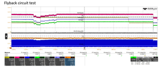
    1) Can you please provide us with some screenshots of the working case.
    How does the system react on the change of the input voltage in a good case?
    I am interested in a change of the FB signal and a change of the duty cycle.
    Plese select the different time scales accordingly.

    2) Together with the FB pin voltage, please also provide the COMP pin voltage

    3) By the way, do you measure the FB voltage on the pins of or device or on the feedback divider resistor terminals?

    4) While the system is in the faulty state, please have a look at all voltages along the resistor-chain R3007, R3008, R3009, R3010 and the FB pin on our device.
    Which of these voltages is changing and which one is static?

    Once the system is in the faulty state, you said that it would return to normal when you power it down for a while.
    5) When the system is in the faulty state, can you please cool it down (with an ice spray or such), so that we can understand if this is a thermo-related effect.


    My only idea how this could happen after a long time is the following:
    Either one of the resistors mentioned above or one of the solder joints of these resistors or of the FB pin on our device somehow loses contact when it heats up.
    Then you have no proper feedback signal anymore and the FB pin settles at 1.3V.

    6) Maybe replace R3007, R3008, R3009 and R3010 and also re-solder the FB pin.


    Best regards
    Harry

  • Hello Harry

    Thank you for your reply.

    1) Can you please provide us with some screenshots of the working case.
    How does the system react on the change of the input voltage in a good case?                                                                                                                   


    2) Together with the FB pin voltage, please also provide the COMP pin voltage

    we will test it .

    3) By the way, do you measure the FB voltage on the pins of or device or on the feedback divider resistor terminals?

    on the feedback resistor terminal 

    4) While the system is in the faulty state, please have a look at all voltages along the resistor-chain R3007, R3008, R3009, R3010 and the FB pin on our device.
    Which of these voltages is changing and which one is static?

    We will try

    Once the system is in the faulty state, you said that it would return to normal when you power it down for a while.
    5) When the system is in the faulty state, can you please cool it down (with an ice spray or such), so that we can understand if this is a thermo-related effect.

    we will try
    My only idea how this could happen after a long time is the following:
    Either one of the resistors mentioned above or one of the solder joints of these resistors or of the FB pin on our device somehow loses contact when it heats up.
    Then you have no proper feedback signal anymore and the FB pin settles at 1.3V.

    I test the FB at R3010 , if loose contact ,how it can settles at 1.3V? 

    6) Maybe replace R3007, R3008, R3009 and R3010 and also re-solder the FB pin.

    Thank you for your advice ,and we will try .

  • Hello Haixian,
    Thank you for the screenshots.

    So, in the "good" case, does the FB signal not change at all when the input voltage jumps up (as this is the quicker change)?
    Is the duty cycle the only thing that changes there?

    Anyway, looking at the unusual case again:
    You see all aux signals changing.
    Therefore, along that chain of resistors R3007, R3008, R3009, R3010) the voltage of this signal should get more and more divided down.
    But the basic shape of that signal should always remain the same.

    In your system, instead, the FB signal is static, and this is not expected.

    The 1.3V will be driven by the COMP pin and "reflected" on the other side of the compensation network.

    So, once you are able to reproduce the problem again, please go down this resistor chain and verify where the signal shape is "lost" and ends up in these static 1.3 Volts.

    Thanks and regards
    Harry