Because of the Thanksgiving holiday in the U.S., TI E2E™ design support forum responses may be delayed from November 25 through December 2. Thank you for your patience.

This thread has been locked.

If you have a related question, please click the "Ask a related question" button in the top right corner. The newly created question will be automatically linked to this question.

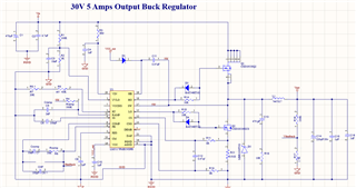
LM5117: Vout drops on connection of load

Part Number: LM5117

Hello TI, 

I am having a challenge understanding what is causing teh volateg at teh ouput to drop from 30V to 0v, when i dissconnect load after the voltage slowly raises back upto 30.6V. My Vin is 36V. 

Volatge mesaurements. UVLO pin - 4.6V, SS pin 4.5V, RES 0v, FB 0.8V Ramp 0V. After conncetion of load UVLO pin - 4.6V, SS pin 0V, RES 0.6v, FB 0V Ramp 0V.
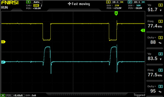
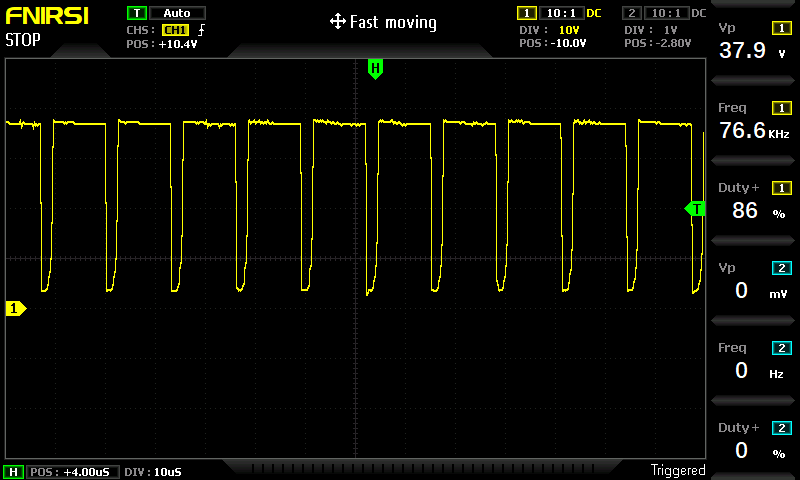
Situation below at the Sw node SW
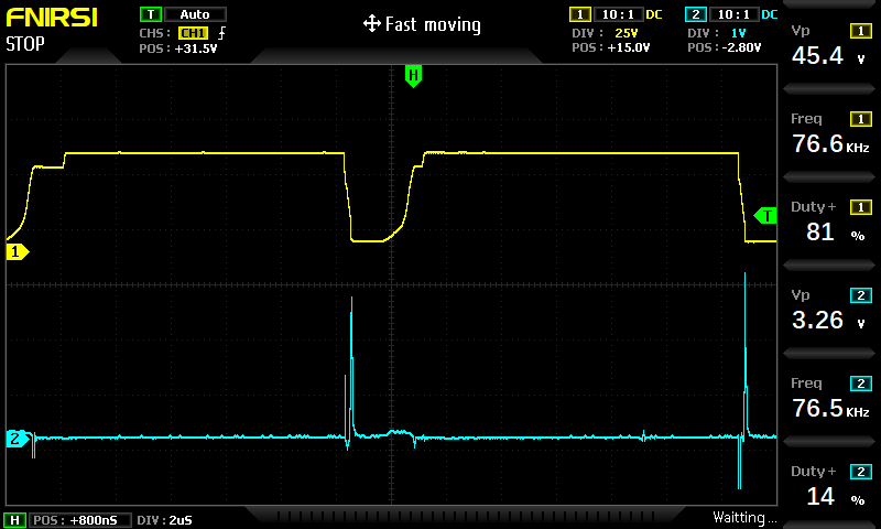
yellow is high side and blue is on the low side switch 
Please advise me on way forward

  • Hello Nasser

    It lseems the converter enterred the hiccup mode protection based on the RESpin voltage measurement.   Please check these items.

    • Please download the Quick Start, and compare your compenent selections with Quick Start recommendations
    • C12 is larger than typical value. Please try 100pF
    • Please check the deatime is enough over VIN and IOUT.    

    -EL

  • Hello Eric, 

    please could you guide me , how can i confirm that the deadtime over VIN and Iout ?

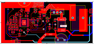
    Also, Do you think my attached layout would help in trouble shoioting this. Is the distance from teh Rs far from the conroller. 

    I have attached my calculator values , i can confirm that all my placed compaonnets are same unless for values that are not standard i have put the closest valu to these. 

    confirmed values.pdf

  • Hello Nasser

    Please use two differential probes, one measures the voltage between the gate and the source connections of the high-side MOSFET, the other measures the voltage between the gate and the source connections of the low-side MOSFET. Please make it sure to match the propagation delays.  

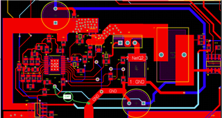
    You need to populate a SMD ceramic capacitor between the drain of the high-side MOSFET and the ground connection of the RSENSE in order to make the switching loop as small as possible. 

    Please locate C12 as close to the IC 

    GND traces are too thin...

    Please check your component values. You are using 22uH while the component selection in the Quick Start is 100uH. 

    -EL

  • Hello Eric, 

    Unfortunately for me, i don'th have diffefrential probes to carry out the test you last suggested. 

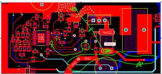
    However i have managed to get a fix to the issue. I solder an electrolytic cap and ceramic close to teh Vout line heading to the feedback configuration of the chip as indicated below and i am able to get stable perfomance of the chip 

    below is when i am loading it whith a 70 watts load (30.6V out and 2.57A)

    I however later had it burn when i connected a battery for charging , I guess its beacause its currently in CV mode and teh battery is Lithium