This thread has been locked.

If you have a related question, please click the "Ask a related question" button in the top right corner. The newly created question will be automatically linked to this question.

UCC28061: Power MOSFETs blown up sometimes

Part Number: UCC28061

Dear TI Team,

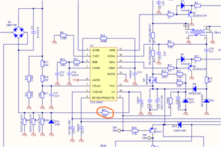
We've encountered an issue with our design that employs the UCC28061 with two power MOSFETs, which are experiencing occasional failures.

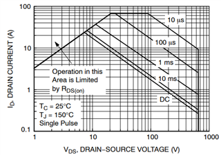
Originally, we utilized the STP25NM60ND MOSFETs for this purpose. However, since this MOSFET has become obsolete, we attempted to replace it with a similar, even stronger MOSFET. Surprisingly, this change led to an increase in failures from 0.5% to 10%.

Upon receiving RMAs back from our customers and attempting repairs by replacing the MOSFETs, we've noticed that the circuit may not function properly afterward. Despite conducting extensive investigations into the circuit, we've been unable to pinpoint the root cause of the issue.

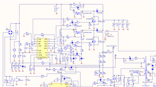
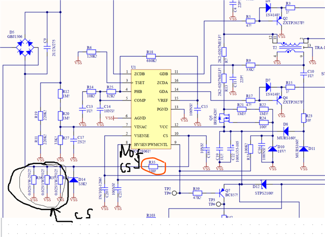
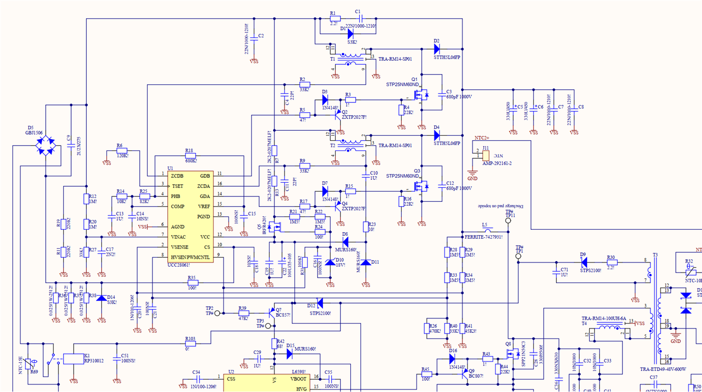
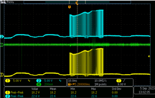
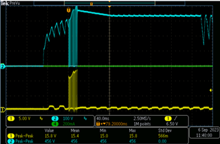
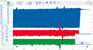
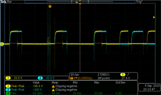
I've attached a section of the circuit below for reference. As depicted, the MOSFETs Q1 and Q3 are the components most frequently affected by failures.

I'm reaching out to gather your insights and expertise on this matter. Perhaps other customers have encountered similar issues, although I haven't been able to locate any relevant discussions in the TI forum. Given that we've been using this circuit design for over 11 years and have continued to sell it to our customers, it's concerning to see the rise in RMAs recently.

Your input would be greatly appreciated.


  • Hello,

    MOSFETs generally fail due to over heating, over current and over temperature.  You had mentioned the design was working fine for a 11 years and when you changed the STP25NM60ND FETs the new FET's get damaged.  You might want to compare the data sheets of the old FET and the new FET you used.  Looked at maximum, current, voltage, Rdson, Coss and gate capacitance.  There is something different about the new FETs that are causing them to fail.  There is something different causing them to fail.

    When companies obsolete FETs sometimes they give a recommendation of a FET you can use instead.  You might want to see if the manufacture recommends a suitable replacement and try the FET they recommend.

    When selecting a FET replacement you typically would like to find a FET with the following qualities:

    - Rdson = or < old FETs Rdson

    - Coss = or < old FETs Coss

    - Ids(typ) and Ids(max) = or < old FET's Ids(typ) and Ids(max)

    -Vds(max)  = or > old FET's Vds(max)

    -Qg = or < Old FET Qg


    Regards,

    Mike

  • Hi Mike,

    Thanks for your prompt reply.

    I'm already familiar with these consideration and specifications of the MOSFET, and as I mentioned earlier, the new MOSFET has even better specifications than the original one.

    Interestingly, the original MOSFET works fine, but we still observed a 0.5% failure rate, and occasionally, even the original one blown up.

    However, the new replacement MOSFETs seem to be performing worse in comparison, and we have more failure (5-10%)

    Most of the failures occur during startup and don't seem to be caused by overheating or excessive current. I'm beginning to suspect that there may be an underlying design issue contributing to this problem. That's why I'm reaching out to you for assistance and expertise in identifying and resolving any potential design issues.

    Your insights and assistance would be greatly appreciated.

  • Hello,

    This seems more like an issue of the FETs not being as robust as the last FETs that you had chosen for your design. 

    You might want to review the maxim peak current, rms current and voltages the FETs are being exposed to and evaluate the worst thermal conditions of the FETs to see if the max ratings are being exceeded.  Even though the original FETs did not fail they may not have been selected for the proper max ratings.

    Regards,


  • Hi Mike,

    I am not sure whether you read my previous text carefully!
    As I mentioned even in original FET there was 0.5% failure as well, the FET seems quite ok (Voltage VDS 600V, enough current, avalanche energy is good enough and so on) I want to know do not you suspect the design???

    It might inherently issue with design!

    When we investigated about the failure, we figure it out the UCC28061 and Q2, Q4 damaged as well as Q1, Q3.

    1. Could you please check the GDA, GDB passes to see whether they are correct or not?

    2. Is the Choke polarity ok? Is it important?

    3. The Choke information is also attached here, I am doubting about the resistor values R2, R9, are they correct?

  • Hello,

    Could you tell me what the peak current limit is set for on the CS pin and what the peak current limit rating is of the FETs?

    Under worst case conditions a single FET could see the full current limit set by the CS pin.  This means that the FETs should be selected to handle this full current.  I have a feeling that the FETs may not have been selected for this peak current and that may be why they are failing.

    Regards,

  • Hi,

    The current sense is 100R, as you can see in the attached schematic.

  • Hello,

    Could you tell me what the peak current limit is set for on the CS pin and what the peak current limit rating is of the FETs?

    Regards,

  • Hi,

    The current sense is 100R, as you can see in the attached schematic.


    For the FET, I can see in the final product, it has been used a similar FET from "onsemi", it is  NTP125N65S3H


  • Hello,

    I double check the schematic.  What you circled is actaully a low pass filter resistor.   The low pass filter is formed by R35 and C18.

    Your current sense resistor is actaully not the current sense resistor.

    Your current sense resistance is actually 0.025 ohms/3 = 8.33 mohm.  The peak current limit is set to 0.2V/8.33 mohm = 24 A.

    So the FETs should be protected during inrush I would think.

    I reviewed the schematic again.  Could you tell me what the "!" marks are?  They are not on all the components.  On thing that could can issue in the design is if D1 is not present.  This component is marked with !.  Could you double check to make sure they are using this inrush diode in there design.

    Regards,

  • Hi Mike,

    Thanks for your checking,

    The ! marks for internal use, you can neglect them.

    What do you mean with this " this inrush diode in there"

    The Diode D1 is definitely present.

    What do you mean of the " this inrush diode in there"?

  • Hello,

    If the inrush diode D1 was not present that inrush current could pass through the boost FETs and would damage them.

    Since it had an ! I thought it may not be present.

    There is something causing those FETs to fail.  Is there anything else in the design that is failing besides the FETs?

    If there is this may give us an indication of what is causing the FETs to fail.

    Regards,

  • hi Mike,

    As I said, Most of the time the MOSFETs are blown up, but sometimes we saw the UCC28061 and Q2, Q4 damage as well.

  • Hello,

    Your inquiry has been received and is under review.

    Regards,

  • Hello,

    When it comes to Q2, Q4 and the UCC28061 failing, it is most likely caused by Q1 and Q3 failing first.  When these FETs fail they will pass high voltage through the gates to lower voltage devices.

    I reviewed the schematic and I am wondering if your low pass filter formed by R35 and C18 to see the CS pin is causing a delay that is defeating your over current protection or delaying it.  This resistor and capacitor has an RC time constant of 1 us.  Worst case this would be a 5 us delay before the CS tripped. It may even be attenuating the CS signal as well preventing over current from tripping when it should.

    I would suggest decreasing that capacitor to 220 pf.  This will reduce the RC time constant to 22 ns and speed up the over current detection.

    Regards,

  • Hi Mike,

    Thanks for the investigation,
    I will try to change the capacitor to see what would be happened. 
    I think any changes need to prove it, but how we can prove to see if it works or not, it would be difficult.

  • Hello,

    You actually should study the CS signal at the CS pin, the voltage across the current sense resistors and current through the FETs with an oscilloscope and current probes before making any changes.  This will give you an indication at what's going on.

    I would recommend evaluating these signals at power up, startup and load transients to see what is happening.  This may give you an indication on why the FETs are failing.

    You also might want to evaluate VCC and the gate drive outputs to make sure that the absolute maximums or minimums are exceeded.  If they are these could cause the controller to fail as well.

    Regards,   

  • Yes, I agree.

    We already checked those signals.
    We have already observed some very narrow spikes over the GS (Gate-Source) of the MOSFETs, which they are above the limits of the GS.
    The spikes are sometimes 80V, but they are quite narrow and below 50nS and might do not have enough energy to destroy the FET. Therfore, in this case we tried to place a bidirectional TVS diode on the G-S to cut them, but not 100% successful. 


    Please see below images:

    1. Startup of Gate Q1, and Q3:


    2. source of Q1 (Blue line) and Gate of Q1 (Yellow):


    3. Source Q1, Gate Q1, Gate Q3:


    In the image 3 we tried to use A trigger point above the normal switching voltage of the gate we found there are voltages on the gate present higher than that.

    The graph shows a clear peak on the gate of Q3 that is higher than would normally be present.

    4. We set trigger points to near the max Gate source voltage we can find more peaks that might be a problem for the FET’s. However, while being over the limit they are so thin(fast) that the FET’s did not break.
    The spikes are below 10ns

  • Hello,

    Did you look at the current through the FETs?  I did not see this on your curves. I was thinking that you may see an over current going through them.  

    Also worth mentioning that you are bandwidth limiting your voltage probes.  You may be missing voltage spikes.

    This last waveform you show.  It looks like there is a large negative voltage on the gate.  If this voltage is negative on the drive pins of the UCC28061 it could cause the device to damaged.  We generally recommend that the voltage on any pin not drop down below 400 mV below ground.  To protect the UCC28061 you could always add Schottky rectifiers on the output of the drive pins.  Remember these need to be as close to the Gnd pin and the drive pins as you can get them to  reduce trace inductance.

    Regards,