This thread has been locked.

If you have a related question, please click the "Ask a related question" button in the top right corner. The newly created question will be automatically linked to this question.

LM66200: Reverse current blocking and "activation current"

Part Number: LM66200
Other Parts Discussed in Thread: LM66100, TPS2117, TPS2116

I'm considering LM66200 or LM66100 to OR two battery sources, but want to prevent reverse leakage current in the event that one battery is discharged farther than the other.

The LM66200 has 2 very useful plots showing that reverse leakage current back into Vout and subsequently out of a Vin pin should be in the nA range (though for the plot on the right it looks like they forgot to show the line at room temperature)

So at room temperature, the leakage into Vout with Vout=3.5V should be about 5nA or so. This sounds great.

However under specifications we see this:
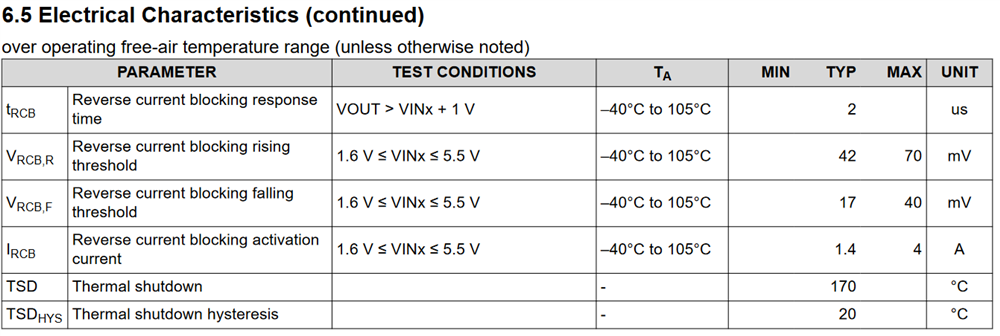
The chart above shows that the reverse current blocking function is "activated" at a typical value of 1.4A or even as high as 4A! What does this mean?

The LM66100 also states that "reverse current blocking" is activated at 0.5A typical and 1.0A max.

If the leakage from Vout to Vin when Vout > Vin is well below 1uA according to the plots, how should I interpret the "reverse current blocking" function?

  • Hi Jim,

    Please see this thread - the IRCB specification only applies to if there is a voltage source on VOUT higher than the VINs which can cause a large current to flow from VOUT to VIN. In this case, current would flow from VOUT to VIN until the 1.4A threshold is reached, in which case both inputs would be disconnected from the output and the output would go Hi-Z. This is where the figures you posted are applicable. However, during normal operation when VOUT is not greater than the active VIN, the device compares the input voltages and outputs the highest one, and the inactive input is disconnected from the output and other input. The inactive input has 50nA typical leakage into VINx.

    During switchover, the active source is first disconnected from the output, then tSW time (on the order of 10us) after the other source is connected. This prevents any cross conduction between the channels from occurring.

    Similarly, with LM66100, if CE > VIN, the output goes Hi-Z. However, if you need this device to start blocking reverse current only once reverse current starts flowing (this is where the 0.5A is relevant), then CE must be connected to VOUT - this is the only way that LM66100 can detect reverse current. This feature is integrated in LM66200.

    In essence - the 1.4A and 0.5A reverse current thresholds are only applicable if your VOUT is being driven at a higher voltage than your inputs. There will be no current flow between inputs.

    Also, thanks for pointing out the lack of room temp trace on the second figure! I will see if we can get that updated in the next data sheet revision.

    Thanks,

    Patrick

  • Patrick -  thanks for your thorough reply.

    So is the left leakage plot under section 6.7 assumed to be the leakage AFTER the reverse current blocking function has been activated and both inputs are disconnected? This is maybe what was not clear, as it does state that one of the Vin inputs is 0V and therefore lower than Vout, but makes no reference to the IC state and if RCB has been tripped.

    If this is all the case, the part will not be a candidate as I need to block very low reverse currents (<10mA) in my specific battery chemistry

  • Hi Jim,

    Yes, that's correct - the figures are taken when there is a voltage source on VOUT, VIN1 is pulled to GND, and VIN2 is floating, so RCB is active. Thanks for your feedback, I'll see if we can make this more clear in the next data sheet revision as well.

    If you have a voltage source on VOUT that you'll need to block <10mA reverse currents from/to your batteries, I have two recommendations:

    1. Use a blocking diode on VOUT - but that somewhat defeats the purpose of using a dual ideal diode.

    2. Use a precision comparator(s) to compare VINs to VOUT with the output connected to the ON pin, and when VOUT > VIN drive the ON pin high, disabling the device. This should disable the device at reverse currents below 10mA.

    Do you think any of the above could work?

    Thanks,

    Patrick

  • The 2nd suggestion is what I am actively exploring, but I have concerns with false tripping a fully discrete protection like this considering transients and the ESR of the batteries causing momentary voltage dips. I also have concerns with tripping during rhe battery installation process as they will be installed individually 1 by 1. These mean the protection probably cannot be latching. It will also need to be tuned with some Rs and Cs to implement the proper delays. 

    Thanks for your support, it’s good at least to know that we have arrived at a similar answer on the discrete comparator solution.

  • Hi Jim,

    Apologies if I am repeating myself, but in order to have the most efficient path forward in your design I'd like to make sure that you'll be having a voltage source on VOUT that will be higher than both the VINs that you need protection against.

    There shouldn't be any false trips when the batteries are being installed (unless there is that voltage source on VOUT). And, the ON pin/RCB state is not latching, LM66200 will resume normal operation when ON goes low/VOUT drops to just above VIN.

    Yes, if going the comparator route, then I think the Rs and Cs would provide good deglitching to avoid tripping during load transients.

    Please let me know if I can clarify anything or if you have any questions or issues here.

    Thanks,

    Patrick

  • Patrick - no worries and I appreciate you following up.

    Here is the gist - I am using 2 LiSOCl2 primary cells in a 1S2P configuration but NOT in a pack. It's possible for installers to place EITHER cell in backwards, or mix an old (fairly discharged) cell with a new cell. The risk here is that new cells will charge old cells.

    The nominal discharge current in my application is about 10mA, peak 30mA.

    The max CHARGE current I have been told is safe for this chemistry by the battery supplier is 10mA. Any more for extended periods of time is a fire/explosion risk. I'd prefer to stay well below this.

    There is no obvious TI solution I can find for this chemistry to protect against reverse current, let alone reverse current AND reverse polarity orientation without severely impeding typical usage efficiency. I think the best option I've arrived back to is a very low Schottky barrier small signal diode with Vf~150mV @10mA best case condition.

  • Hi Jim,

    Thanks for the explanation - in this case, provided that the batteries aren't directly shorted together then LM66200 (or TPS2116/2117, which are very similar but feature more control options) will certainly work here. There is no risk of a new/higher voltage battery discharging into the old/lower voltage battery, either internally or through VOUT. But unfortunately, this device does not have reverse polarity protection. Either discrete diodes or ideal diodes will work here if you need reverse polarity protection - but ideal diodes usually have higher Iq and a higher minimum VIN.

    Thanks,

    Patrick

  • Patrick - can you elaborate?

    You said "There is no risk of a new/higher voltage battery discharging into the old/lower voltage battery, either internally or through VOUT." but the reverse current blocking function states it will allow up to 4A max reverse current to flow in LM66200 before activating RCB. Can you explain?

  • Hi Jim,

    Sure - what the IRCB spec describes is that, if there is a voltage source that is only on VOUT (not through the inputs) from which a source flows back into the active input (the inactive input automatically blocks reverse current), then when 1.4A typ, 4A max flows from the VOUT source to the active VIN, then the device will disconnect both inputs from the outputs and make the output Hi-Z. So it only applies if you have a third power source on VOUT, and it doesn't apply if you are only powering your circuit from the sources on IN1 and IN2.

    The device determines which output to use by comparing VIN1 and VIN2 - it connects whichever source is higher to the output. When the device switches from one input to the other, it goes as per the following example where the device is switching from VIN1 to VIN2:

    -VIN1 active, VIN2 inactive (so VIN2 is blocking all current in and out of the IN2 pin except 50nA leakage into the pin)

    -VIN1 disconnects from VOUT (so that it blocks all current except 50nA leakage into the pin), VIN2 is still inactive

    -After tSW (around 10us), VIN2 connects to VOUT

    As you can see here, there is no possible situation where VIN1 and VIN2 are both connected to VOUT at the same time, or connected to each other. (It's also worth mentioning here that this device cannot have both inputs enabled at the same time like you would see in a real dual diode when both inputs are the same voltage.)

    So, in essence - the device selects which input to connect to the output based on the voltages of the inputs, not based on how much reverse current goes through a channel. As per the device design, only one channel can be active at a time. If there is a voltage source on the output that is greater than both inputs, current will flow from the output to the active (highest) input - if 4A max flows from the output to the input in this condition, then the device will disable the active input so that both inputs are disconnected from the output.

    I can see from the data sheet how it can be confusing - does that make sense? Do you have a third voltage source on your output - one that is not the IN1 or IN2 supply?

    Another perspective to look at this from is by looking at Table 7-1 of TPS2117 data sheet, in the row titled "Diode Mode." This is a very, very similar device that expands the control modes of LM66200, but the Diode Mode is the same operation as LM66200's operation.

    Thanks,

    Patrick

  • Patrick,

    I believe I understand now.

    My system does not have any external source on Vout.
    The only sources in the system are two separate LiSOCl2 batteries with nominal voltage of 3.6V, one connected to each of the VIN inputs.
    I would prefer if both cells were equally loaded, but realize that this may not be realistic for how the IC functions (or even with external Schottky's for that matter). The cells will be connected 1 at a time individually, with separate reverse polarity protection.

    I ran a transient analysis in PSPICE for TI:

    I indeed see no leakage current from Vout to VIN when trying to wiggle around each input using VPWL, but I can't speak to how robust the LM66200 model actually is to demonstrate this.

    Can you confirm my understanding of how this would likely work would be the following, stepping in time as if you are inserting each battery cell:

    Some (hopefully final!) questions:

    1. Is the system above clear?

    2. The datasheet is also not clear what the changeover threshold voltage is between Vin1 and Vin2. Is there a changeover threshold for when Vout is connected to one input over the other? Is there hysteresis?

    3. As the batteries are discharged and ESR increases, is it reasonable to think the IC may "flutter" back and forth between sources if transients cause intermittent dips in input voltages? I imagine this could happen, we would obviously need to test.

    4. Given the system explanation above, is it correct that we will expect <=50nA of leakage back into each battery cell as there is truly no external source connected to Vout?

  • Hi Jim,

    While I'm not familiar with the internals of the simulation model as I did not make it, it is accurate in portraying the no leakage from VOUT to VIN.

    Yes, the table you posted is exactly correct.

    1. Yes, looks great!

    2. There's no hysteresis or threshold on the input comparator, so it is very sensitive.

    3. Yes, this can happen and in severe cases it can cause the IC to go into soft start and/or a system reset because the output drops to far. If this turns out to be an issue (or if you want to proactively avoid this possibility), this can be mitigated by adding capacitance on the inputs so they droop less when they're connected or it can be prevented by using the previously mentioned parts, TPS2116/7, which can be programmed to use Battery 1 until it reaches a threshold of your programming, after which it switches and uses Battery 2 until Battery 1's voltage is high enough (both the falling and rising thresholds can be programmed). But most of the time we don't see this "fluttering" issue to be bad, especially at lower load currents.

    4. Rather, the leakage is from VIN2 to GND, not VOUT to VIN2 - but yes, <=50nA typ (up to 2.1uA max at 105C) leakage into the inactive input. I believe there is only leakage coming out of VINx when it is below 1.6V, as otherwise it will be sourcing the 50nA - but I'm more confident in the concept of this than the exact voltage the input would stop sourcing and start sinking, though.

    Best in the rest of your design! Please don't hesitate to reply here or start a new thread if you have any more questions.

    Thanks,

    Patrick

  • Patrick - so we would expect it to switch from Vinx to Viny when there is a difference of 1mV, 1uV etc? There is no threshold aside from I'm guessing the tolerances of comparator offset voltages etc.

    Thanks again for all of your support this is all very clear now.

  • Hi Jim,

    That's correct.

    Thanks,

    Patrick