


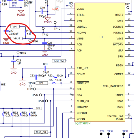
I am looking at the schematic for the BQ25731EVM module, and I see that there are net labels for VIN and VBUS, and PGND and GND.
For VBUS and VIN, it appears they are tied together with a 1ohm resistor, near the VBUS pin:
As for the PGND and GND, that looks like it is tied together using a net-tie. Not quite sure what that is as I am still decently a beginner at circuit design:
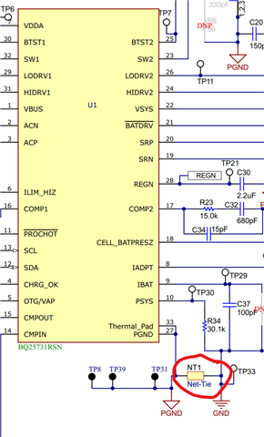
That part is not listed on the BOM either, which is more confusing.
Additionally, what is the purpose of Q7 and (what appears to be) Q6? Actually, what is the purpose of this whole region:
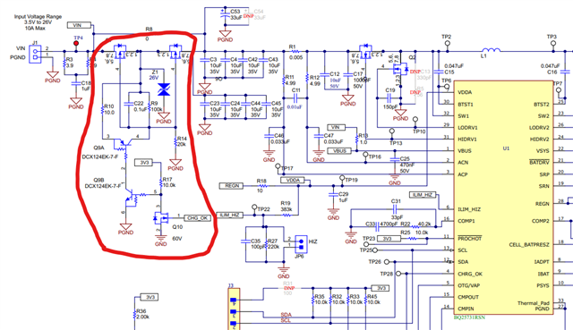
If I had to make a guess, it only allows current to flow if CHG_OK is true, which would be true if the battery is connected?
Thanks for the help!
Datasheet for quick reference:

