This thread has been locked.

If you have a related question, please click the "Ask a related question" button in the top right corner. The newly created question will be automatically linked to this question.

LMR62421: Generating both +5,5V and - 5,5V Output Voltages from single 3v3 Positive Input Voltage

Part Number: LMR62421
Other Parts Discussed in Thread: TLV61070A, TLV61048

Hi, this is volkan
Greetings from Istanbul.
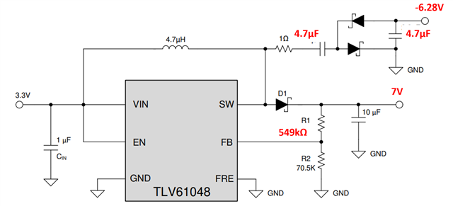
In my application I need these two fixed DC differential voltage sources to pass the rail to rail level in an opamped circuit where I will drive peak to peak +-5V DC

In order to supply these fixed differential 5V5 DC Supply which I need to feed for the op amp, i am looking for to design Boost/SEPIC Conversions design with Effective, simple and cost friendly way.

I wonder if I can get a total supply of 400ma for +-5,5V and 200ma for -5,5V  from single 3V3 DC source with this single simple switcher ? If yes could you please guide me how to i do that ?
I would appreciate if have any examples, design notes or calculation formulas.
If i can not able to get these differential source from single 3v3 then which component is suitable to my application ?
Thank you for the support.
Best Regards
Volkan

  • Hi Volkan,

    Sorry I'm a little confused. Do you mean you'd like to generate +5V/400mA and -5V/200mA outputs from a +3.3V source?

    What's the biggest gap between the amplitude of the +5V and -5V that can be accepted? For example, is +5V and -4.4V OK?

    One possible solution is the topology shown in this APP NOTE(click here)

    You may take a look at first. If it's OK, we can further finetune this solution with more suitable device.

    Regards

    Lei

  • Hello Lei, thank you very much for your response with valued information.
    I believe your understanding is correct, i would like to specify the output voltage ranges again.
    Positive side average current 400mA Supply; Any value between +5.5V and +6V
    Negative side average current is 200mA Supply; It can be any value between -5.5V and -6V as well. And the gaps between the amplitudes are not sensetive
    My input source is +3.3V and capable 4A current.

    The application note you mentioned is a good example but the maximum current it can give is 100ma limited.
    If you can able to provide further finetune solution with more suitable device i appriciated,

  • Hi Volkan,

    If max +5.5V or -5.5V is OK, then TLV61070A can be the choice.

    If the Vout must reach +6V or -6V, we need to further check available device.

    Just let me know if there are any other detailed requirements, which is helpful to narrow down the best choice.

    Regards

    Lei

  • Hi Lei, thank you for your quick response.
    Yes, these two voltages +5.5V and -5.5V are suitable for me if can able to get a constant output at as long as it can deliver the desired currents. Because due to input offset voltage Characteristic of the opamp +-5.4V is the limit value for me it should not fall below this value . Limit value so close to +5.5V or -5.5V voltage range What do you recommend ? If TLV61070A will not drop under +-5.4V then i can able to use it.
    Edit: By the way, my maximum upper amplitude limit is +8v to -8v.

    If TLV61070A will not drop to limit values and would supply currency which i need then Please let me know, i do need to use same method which you previously provided by application Report to supply these differential voltages ? Any guide i appriciated.
    Thanks
    Volkan

  • Hi Volkan,

    When TLV61070A is used and the max Vout is +5.5V, the -5.5V is hard to be achieved since the gap between the positive and negative output caused by the charge pump topology. The negative output may be like -4.7V. As your information, it should be not acceptable.

    As you pointed, the maximum upper amplitude limit is +8V to -8V. So I think we can go back to the device of TLV61048. It's Vout can be configured to 7V. Without any additional components to eliminate the gap between the positive and negative output, the negative output can be around -6.3V, with enough margin.

    In the APP note, 100mA is the max Iout of the application example, not the limitation of TLV61048. It can output 400mA and 200mA.

    Regards

    Lei

  • Lei, thank you for your valued informations. Everything is clearer to me now.
    One last think i need to confirm.
    According to the schematic in the application note, what values do you recommend me to use in such a current output ?
    Especially D1,D2 and D3  What do you think these schottky diodes should be ?  Schottky diodes B120AF-13 ok for all ?
    Also RCHG and CCHG values should it remain the same as Figure 5 in the application note ?
    Finaly Thanks for the help
    Regards
    Volkan

  • Hi Volkan,

    Here is the recommended component values for the application. The final values may be adjusted based on the finetuning on the actual board, but they should be good start values.

    The two diodes in charge pump part(no device ID) can be normal Schottky diodes.

    The diode D1 can either be the same Schottky diode, or normal diode with higher forward voltage(which will make the amplitude of negative Vout more close to the positive Vout but with more power loss), it depends on customer's preference.  

    Regards

    Lei

  • Lei
    Thank you for your support. Everything is clear now.
    Best Wishes
    Volkan