This thread has been locked.

If you have a related question, please click the "Ask a related question" button in the top right corner. The newly created question will be automatically linked to this question.

TPS65220: PMIC features understanding

Part Number: TPS65220
Other Parts Discussed in Thread: AM6412, TPS22965, TPS6521905

Hi All,

I have to study the most compact possible solution powering a SITARA AM6412 and I found some PMIC references that may be could suit the situation.

( the only interfaces w'ill use are QSPI,PCIE,UART)

Here are some questions about TPS6522053 and 65219 variants(from 01 to 08, plus 0C).

1 - Because there are a lot of variants, is there a document explaining the differences between this parts ?(the SLVAFE9 stops at 6521904) ?

2 - Can you explain the purpose of the FSD feature that is enabled by default on TPS6522053, and TPS6521901 to 04. 

   - does "first" mean : first time the part ever sees the power, or does it mean every time it sees the power therefore bypassing the EN input signal control (we DO want an enable control) ?

  - Perhaps FSD only applies to the I2C function which has to be operational continuously and not the DC/DC and LDO functions. Please explain.

3 - Among all the variants is there one that can be programmed "at home" ?

4 - how can we disable FSD for parts where this feature is by default enabled  and which are not programmable at home ?

 5 - What would be wrong when using the 3V3 LDO1 output to source the AM6412 3V3 pins such as VDDSHV_MCU and others (considering total current < 400 mA)  ? All the examples use an additional TPS22965 

6 - Can you explain the concept of "Bypass" versus "load switch" relative to LDO1? . Isn'it the same when LDO-VIN=3,3V and we want LDO-Vout=3,3V ?

7- Supposing LDO-VIN = 3.3 and LDO1 configured in bypass mode(default) should we expect LDO1-VOUT be equal (worst case) to 3.3-0.2*0.4 (due to Bypass resistance) = 3.22V ? or should we consider we loss at least 300mV dropout ?

8 - Same question when LDO1 configured in load switch mode : only 0.2 Ohm Rswitch has to be taken into account ?

9 - in the SKAM64 EVM we can notice that LDO1_VIN=3.3V expecting LDO1_VOUT=3.3V despite the "by_default" bypass mode of the TPS6522053. How is this managed ?

With best regards,

Bruno

  • Hi,

    Thank You for using E2E. Please find our feedback below and let us know if there are any questions.

    1 - Because there are a lot of variants, is there a document explaining the differences between this parts ?(the SLVAFE9 stops at 6521904) ?

    [TI] There are new variants that have not been added to the AM64x Apps note yet. The comparison between all the existing variants for AM62x and AM64x can be found on table 3-1 (page#5) of the following Apps note: https://www.ti.com/lit/pdf/slvafd0

    4 - how can we disable FSD for parts where this feature is by default enabled  and which are not programmable at home ?

    [TI] When the FSD feature is enabled, the state of the EN/PB/VSENSE pin is ignored only during the first power up when the PMIC goes from "NO Power" to "Active". Once the first power-up is complete and nRSTOUT is released, the PMIC will start monitoring the EN/PB/VSENSE.  

    3 - Among all the variants is there one that can be programmed "at home" ?

    [TI] Yes, the TPS6521905 is the user-programmable version. It comes with all the rails disabled by default and allow customers to configure a custom NVM configuration. The programming guide can be found in the product page at the following link: https://www.ti.com/product/TPS6521905

    4 - how can we disable FSD for parts where this feature is by default enabled  and which are not programmable at home ?

    [TI] The FSD setting can be changed by writing to register field "PU_ON_FSD" on address 0x20, bit#7. Pre-programmed devices that have FSD enabled do not allow to make any NVM changes before the power-up sequence is executed. The user-programmable version (TPS6521905) allows to configure custom NVM settings for a lot of register fields including the FSD.

     5 - What would be wrong when using the 3V3 LDO1 output to source the AM6412 3V3 pins such as VDDSHV_MCU and others (considering total current < 400 mA)  ? All the examples use an additional TPS22965 

    [TI] The processor spec for the sequence requires the 3.3V supply to ramp up first and most of the PMIC variants have LDO1 ramping up after the 3.3V rail. A custom NVM configuration might allow to use LDO1 for the 3.3V IO domain if the sequence and settings are configured accordingly.

    6 - Can you explain the concept of "Bypass" versus "load switch" relative to LDO1? . Isn'it the same when LDO-VIN=3,3V and we want LDO-Vout=3,3V ?

    [TI] Bypass allows switching the rail config between load-switch and a fixed 1.8V LDO. For example, some of the PMIC variants have the LDO1 configured as bypass and the output voltage set by the VSEL_SD pin with the following polarity:

    • VSEL_SD High, LDO1=3.3V (behaves as bypass, similar to load-switch and requires PVIN_LDO1=3.3V)
    • VSEL_SD Low, LDO1=1.8V (behaves as a fixed 1.8V LDO)

    7- Supposing LDO-VIN = 3.3 and LDO1 configured in bypass mode(default) should we expect LDO1-VOUT be equal (worst case) to 3.3-0.2*0.4 (due to Bypass resistance) = 3.22V ? or should we consider we loss at least 300mV dropout ?

    [TI] The dropout when configured as bypass would be 200mOhms (or 250mOhms) multiplied by the current.

    8 - Same question when LDO1 configured in load switch mode : only 0.2 Ohm Rswitch has to be taken into account ?

    [TI] Yes, 0.2Ohm or 0.25Ohm depend on the input voltage.

    9 - in the SKAM64 EVM we can notice that LDO1_VIN=3.3V expecting LDO1_VOUT=3.3V despite the "by_default" bypass mode of the TPS6522053. How is this managed ?

    [TI] When PVIN_LDO1=3.3V, the output of LDO1 would not be exactly 3.3V. VLDO1 would be 3.3V minus the dropout which is based on the output current and internal FET resistance. The output voltage is labeled as 3.3V for simplicity,  because the exact number will depend on the current consumption. 

    Thanks,

    Brenda

  • Hi Brenda,

    Thank you for your quick reply.

    However there are still some dark areas

    2 -  first  power-up means :

        - first power-up (PVIN detection) after device manufacturing ? or 

        - each time the PVIN comes from "not detected" to "detected" state ? therefore meaning that every time that the board is powered-off then powered-on all           Vout outputs will appear independently of the EN_PB_SENSE input ?

    2b - What would you suggest to prevent All Vout to establish (respecting the sequence order) untill a trigger signal is applied.

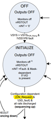
    2c - In the state diagram figure 7-10 I could not find any reference to FSD. The "ON REQUEST" permitting to enter the active state doesn not depends on FSD. Should'nt it be the case ?

    10- in the SITARA AM6412 datasheet there is the figure 7-5 showing power-up sequence to respect but I could not find any timing value specifying the required delays between rails. Where can we find this information ?

    With best regards,

    Bruno

  • Hi,

    Please find our feedback below and let us know if there are any questions. 

    2 -  first  power-up means :

        - first power-up (PVIN detection) after device manufacturing ? or 

        - each time the PVIN comes from "not detected" to "detected" state ? therefore meaning that every time that the board is powered-off then powered-on all           Vout outputs will appear independently of the EN_PB_SENSE input ?

    [TI] First power up means every time the voltage on the main supply (VSYS) goes above the POR threshold. Every time the PMIC goes from "No Power" to "Active State". 

    2b - What would you suggest to prevent All Vout to establish (respecting the sequence order) untill a trigger signal is applied.

    [TI] To prevent the PMIC from ignoring the state of the EN/PB/VSENSE pin during the first power-up, I would recommend using the user-programmable version (TPS6521905) with a custom NVM config and FSD disabled. Just for our reference, what is the concern with using one of the existing variants that have FSD enabled? We have not seen any customer who is using AM64 or AM62 reporting an issue with the FSD feature. 

    2c - In the state diagram figure 7-10 I could not find any reference to FSD. The "ON REQUEST" permitting to enter the active state doesn not depends on FSD. Should'nt it be the case ?

    [TI] When FSD is enabled, the "ON REQUEST", highlighted in the diagram below, is ignored during the first power-up.

    10- in the SITARA AM6412 datasheet there is the figure 7-5 showing power-up sequence to respect but I could not find any timing value specifying the required delays between rails. Where can we find this information ?

    [TI] The AM64 processor just requires the previous rail to have a stable voltage before the next rail is enabled. The MCU_PORz which is driven by the PMIC nRSTOUT does have timing requirements. I would recommend submitting a separate E2E to the processor forum for any questions about the AM64 processor.  

    Thanks,

    Brenda

  • Hi Brenda,

    Thank you for your answers.

    2b : Well , It could be OK considering we are still able to force the SITARA RESET independently of the PMIC RSTOUT. The thing is that I consider strange to provide a feature that is supposed to control the PMIC output but with the exception that it will not the first time. I don't see the purpose of this exception so far. And since it looks strange to me I want to be sure not having missunderstood something.

    5 - Since the 3V3 is the first rail to be applied to the SITARA, why not simply apply the 3V3 VSYS input instead of gating it by GPO2 ?

    With best regards,

    Bruno

  • Hi Bruno,

    Here is my feedback:

    FSD: The FSD help applications that are only controlling the power-down of the PMIC with external logic/ICs. In this scenarios, the PMIC can turn-ON as soon as there is a valid voltage at the input. After that, the external logic/IC takes over and drives the enable pin to trigger a power-down sequence when needed.

    3V3 rail: The external power switch that you see in the power delivery diagram (PDN) is optional because the 3.3V domain is the first rail in the power-up sequence and the last one in the power-down sequence. The discrete power solution doesn't include it. We recommend using the external power-switch to have the PMIC controlling the full sequencing. If the external power switch is not used, then the 3.3V pre-regulator is directly connected to the processor acting as an "always ON" rail and it will not power cycle during a COLD reset or when there is a fault detected on the PMIC. 

    Thanks,

    Brenda