This thread has been locked.

If you have a related question, please click the "Ask a related question" button in the top right corner. The newly created question will be automatically linked to this question.

UCC28951: Primary side MOSFETs' fault

Part Number: UCC28951
Other Parts Discussed in Thread: UCC28950

Hello,

While testing a 2.5kW PSFB design, it is successfully working and giving expected 48V output at 10% load (5.3 A). But as the load is increased to around 8-9A, MOSFETs B and C are getting damaged (all legs shorted). Thus, shorting the input.

Visible burn marks can be seen on the thermal tape of the heat sinks of AB leg. (Indicating B is getting more heated compared to C which was also shorted but had no burn marks on the thermal tape of heatsink).

MOSFETs A and D were fine.

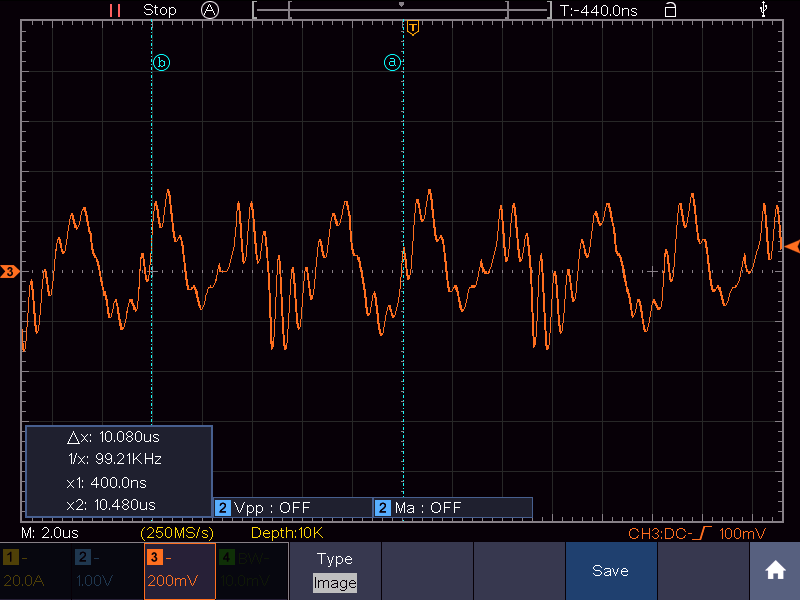
As expected MOSFETs A and B are not operating at ZVS at 10% load, unlike CD leg which is operating at ZVS and is comparatively less heated. 

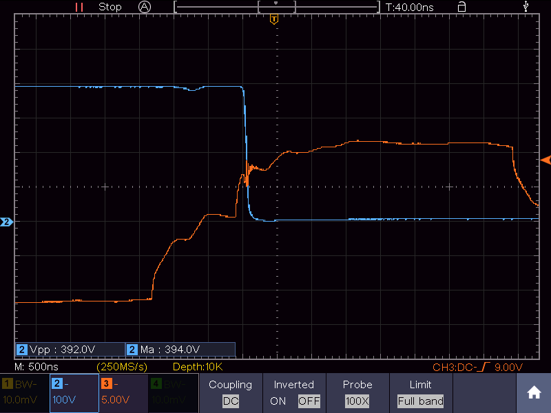
Blue: Vds of MOSFET B;

Orange: Vgs of MOSFET B

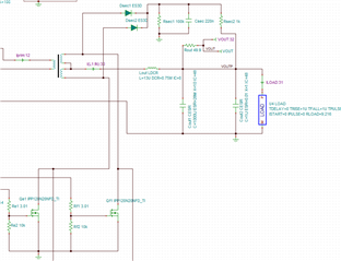
The Primary side MOSFETs used are (IPP65R110CFDXKSA2) and the heatsink used is (SK 481 50 - Fischer Elektronik).

How can the MOSFETs B and C be prevented from getting damaged?

Regards,

Nishant S

  • Hello,

    FETs fail due to over current, over voltage and/or over heating.  You need to determine which one is causing the FETs to fail.  You should study the current through the H Bridge FETs and the primary of the transformer to make sure the current behaves as expected.  I would also evaluate your E and F FET timing to make sure it is correct.

    The following link will bring you to an excel design tool that will go through the step by step design process of a PSFB using the UCC28951.  There also is an excel design tool that goes with this application note, there is a link to it in the application note.  I believe you will find the applications note and design tool helpful.  This information will help you setup FET timings; as well as, calculate component losses and how to setup the controller to help protect FETs from over current.

    https://www.ti.com/lit/pdf/slua560

    Regards,

  • Hello,

    Yes, Excel tool has been taken for reference and the MOSFET has been selected according to the values recommended by it.

    After providing forced air cooling, this time all the primary MOSFETs worked fine (tested up to 9A).

    At current stage, we tested using Schottky diodes (IDH20G65C6XKSA1) instead of MOSFETs on secondary side.

    The snubber calculation was verified by formula from the given link. Snubber Circuit.

    Taking Xmer turns ratio as 6:1:1, and Llk as 0.89uH with peak current of 57.29A (from Excel tool Ips). The RCD snubber circuit selected was Capacitor (0.22 uF), Diode (600V SiC Ultrafast Recovery Diode) and resistor (1kOhms, 35W Arcol).

    Now the problem is after using synchronous 200V MOSFETs (IPP120N20NFD) instead of Schottky diodes. The synchronous MOSFET get shorted in this case (due to high voltage spike). 

    With same snubber the board was giving expected 48V output when Schottky diode were used instead of SR MOSFETs at secondary side. 

    Is the MOSFET getting damaged due to snubber failure. How can the snubber be improved?

  • Hello,

    Have you considered using an RCD snubber on the SRs to protect it instead of a snubber?

    Snubber circuits just dampen ringing.  You might need to add and RCD clamp to protect the FETs.

    Regards,

  • Hello,

    Sorry for the confusion, I was talking about the RCD clamp itself.


  • Hello,

    Thanks for letting me know.  

    Regards,

  • Hello,

    Firstly, even after using RCD Clamp snubber circuit (with values mentioned above) and synchronous MOSFETs (mentioned above). The synchronous MOSFETs legs are getting shorted. 


    For the second test, 650V rated Schottky diodes instead of synchronous MOSFETs are used on secondary side along with forced air cooling. This time at 17% of loading (9A) the primary side MOSFETs shorted (which is also rated for 650V).

    All the below waveforms are at 10% Loading (CR) (5A) (Input Voltage: 400V)

    The CS pin waveform is probed. The waveform does not resemble the one given in application note of UCC28950. 

    Fig. Waveform at CS pin.

    The waveform at the secondary terminals of Current Sense Transformer is given below. 

    Fig. Waveform on the Secondary terminals of Current Sense Transformer.

    Occasionally at the start-up, audible ticking noise can be heard from the board (When the output voltage is being built-up). This is due to Hiccup Mode and is verified by probing on SS pin. Once output is at steady-state, there is no noise.

    Fig. SS pin Waveform at start-up.

    Other times, the soft start is working properly.

    Fig: Waveform of CS pin and SS pin at Start-up at 5A (10% loading)

    Blue: SS pin Waveform
    Orange: CS pin waveform.

    Is there any issue in CS pin signal which is causing the primary MOSFETs to fail?

    Why is the circuit occasionally going into Hiccup Mode? Is there any problem in Current Sense circuitry?

    Regards,

    Nishant

  • Hello,

    Awaiting your response.

    Regards,

    Nishant

  • Hello,

    If your SR FETs are failing.  They are failing due to over current/over voltage and or over temperature.

    I agree that your current sense signal does not look correct.  It also should not be going above and below ground.

    If you are not measuring the primary current correctly with the current sense transformer you will not be able to protect the design and FETs.

    So the first thing you need to do is to figure out why your CS signal does not look correct and fix this.

    The following link will bring you to an application note that goes through the step by step design process of the UCC28951 in a phase shifted full bridge.

    There is a section on how to setup the CS transformer setup.  This should help you double check your CS transformer configuration and setup.

    https://www.ti.com/lit/pdf/slua560

    The following link will bring you to the UCC28950/1 600 W evaluation module's user guide.  You can use the schematic and layout of a proven design.  You can use this schematic and layout as a reference and compare it to your design to see if there are any differences compared to your design.  This may help  you in the troubleshooting process.  You may also want to order this EVM to evaluate the design performance.

    https://www.ti.com/lit/pdf/sluu421

    Until you get the CS signal cleaned up I would not recommend fulling loading the design.  I would also disable the SRs until you have the CS signal cleaned up.

    Regards,