This thread has been locked.

If you have a related question, please click the "Ask a related question" button in the top right corner. The newly created question will be automatically linked to this question.

TPS53353: The voltage fluctuates greatly during use, resulting in damage to the load chip.

Part Number: TPS53353

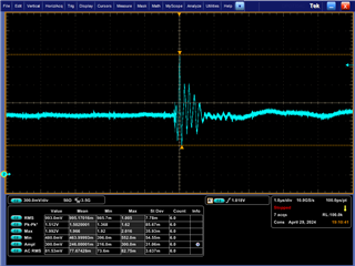
Our company uses 1 piece of TPS53353 to supply power to two pieces of XC7K325T-2FFG900 nuclear pressure VCCINT1V0 at the same time (accuracy ±3%), the total current demand is expected to be about 15A, there is a huge voltage fluctuation(max:2.4V) in the working process, about a few minutes of occurrence, no specific law was found, what is the reason for this, or what causes such fluctuations, how to solve it?

The test waveform is as follows:

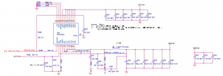
The schematic diagram is below:

Best wishes!

  • Hello,

    Can you explain what the waveform is showing above? Is this Vout?

    Also can you share all your application conditions? Vin? Vout? Fsw? Load is 15A correct?

    Thank you,

    Calan

  • Hi,The above waveforms are Vin=12v, Vout=1V0, FSW=500KHz, Ioutmax=15A, and the power supply supplies power to Xilinx's FPGA core.

  •  

    Looking at the waveform you shared, we are seeing a resonance at 6.67MHz (4 cycles in 3 sub-divisions @ 1μs / division = 150ns per cycle).  With the TPS53353 switching at 500kHz, this is not likely coming from the TPS53353.  If this is happening every few minutes, with the initial pulse being down, there is likely a sudden load pulse drawing energy out of the output capacitor and stimulating a resonance between a layout inductance and some of the output capacitors.

    It is unlikely that the 470μF polymer capacitors or even the 47μF ceramic capacitors are still capacitive at 6.67MHz, so it is more likely the 0.1μF capacitors or some input bypass capacitance at the the XC7K325T-2FFG900 reacting with a layout inductance. 

    1) Check the self-resonance frequency of the 0.1μF capacitors, if their self-resonance frequency is 6.67MHz, or very close, they could be self-resonating.  Instead of 3 identical capacitors, change one from 0.1μF to 0.33μF and the other to 33nF.  This will spread out their self-resonant frequencies without spreading them so far they introduce a inter-capacitance resonant frequency, which may help reduce it.

    2) If you don't find a capacitor you are currently using with a self-resonant frequency at 6.67MHz, you may also look for a small package (0201 or 0402) capacitor whose Self-resonance frequency is very close to 6.67MHz and has a few 200 or more mΩ of ESR to act as a resonant bypass at the input of the XC7K325T-2FFG900.  The 200+ mΩ of ESR will serve to self-dampen the resonance while matching the self-resonance frequency of the capacitor will help it shunt the ringing energy to ground before it can affect the XC7K325T-2FFG900.

  • Hi, thank you very much for your feedback, next we will experiment according to your opinions, for our TPS53353 schematic design I found a few problems, I don't know if it needs to be modified?

    1. The VDD pin does not have a separate 4.7uf capacitor to the ground, but shares the decoupling capacitor with the LL pin, is it necessary to add a 4.7uf capacitor separately?
    2. The LL inductance value is 1uH, and the actual Webench recommended inductance value is about 0.44uH, does the inductance value need to use 0.44uH?What are the effects if you use 1uH?
    3. The decoupling capacitor uses 4pcs*47uf and 3pcs*0.1uf ceramic capacitors, which are placed close to the LL pins.Should the 47uf and 0.1uf capacitors all be removed?
    4. Your company's Design Calculation excel has two red alarms (ESR_min_stability & Vo_undershoot) and I don't know how to design it as a normal value (as shown in the figure below)?
    5. In addition to the above questions, can you help me see if there are any other questions?We look forward to hearing from you, thank you!Best wishes!
  • Hi Shuda,

    The VDD pin does not have a separate 4.7uf capacitor to the ground, but shares the decoupling capacitor with the LL pin, is it necessary to add a 4.7uf capacitor separately?

    Yes the VDD pin should have a dedicated 4.7uF and it should be placed close to the VDD pin during layout.

    The LL inductance value is 1uH, and the actual Webench recommended inductance value is about 0.44uH, does the inductance value need to use 0.44uH?What are the effects if you use 1uH?

    Yes datasheet recommends 1uH so please continue using 1uH. Need to check with WEBENCH on why 0.44uH is being recommended.

    The decoupling capacitor uses 4pcs*47uf and 3pcs*0.1uf ceramic capacitors, which are placed close to the LL pins.Should the 47uf and 0.1uf capacitors all be removed?

    Are these caps placed close to the LL or switch pin in the layout? Is that what you mean? If so, the SW noise can couple into the output. Please follow the datasheet layout guidelines to check if placement is good.

    The output capacitance is actually too large as per datasheet. It needs to be limited to 220uF or lower and a typical value of 3x22uF. So, the E12 and E13 470uF caps need to be removed. This will likely lower the ESR since the 47uF caps look to be ceramic. However, you can add a ripple injection RCC network the values of which can be designed using the design calculator tool.

    Your company's Design Calculation excel has two red alarms (ESR_min_stability & Vo_undershoot) and I don't know how to design it as a

    Looks like the red cell is flagging that the minimum ESR requirement is not met. You need to design and use the RCC injection network across inductor onto FB using the design calculator. 

    Thanks,

    Amod