This thread has been locked.

If you have a related question, please click the "Ask a related question" button in the top right corner. The newly created question will be automatically linked to this question.

UCC256404: Disabling Burst mode resulting in loss of regulation at Output

Part Number: UCC256404
Other Parts Discussed in Thread: UCC28950

Hello,

Background:
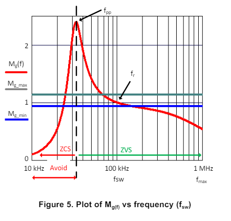
Looking for some design advice in relation to disabling burst mode on the UCC256404. The objective of my LLC convertor is to maintain a 24V output from a 400V input, SWF 90Khz-120Khz with max load 10A. Initial operation in Option mode 6, resulted in burst mode activating in any load condition.   After referring to the 7.4.3.2 section within the data sheet, I have programmed the BW pin to allow for Option 7 ( Burst mode disabled). Following this, I proceeded to test the circuit but found with an input of 180V to be losing regulation in the output voltage and the Switching frequency was capped around 60Khz. 

Question 1
Is there a way to increase the maximum switching frequency within the Burst mode disabled operation? 

Question 2.

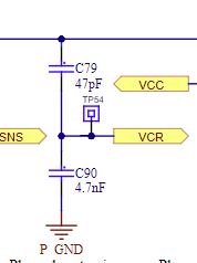
How should the LL/SS pin and the VCR pins be configured when burst mode has been disabled?


Cheers,

Euan

  • Hello,

    I am reviewing your inquiry and will get back to you shortly.

    Regards,

  • Hello,

    In LLC design we recommend that you keep the input range less than 2 to 1.  Your design most likely does not have enough gain to maintain the output voltage.  This could be due to the Lr and Lm ratio or your transformer turns ratio is off.

    The following link will bring you to an excel design tool that you can use to double check your design. 

    https://www.ti.com/tool/download/SLUC675

    In  regards to you design.  If you really need the design to work at an input range of greater than 2 to 1.  I would recommend using a phase shifted full bridge.  Using the UCC28950/1 controllers.  You can design up to a 4 to 1 input range without issue.  The following link will bring you to the UCC28950 product folder.

    https://www.ti.com/product/UCC28950?keyMatch=UCC28950&tisearch=search-everything&usecase=GPN-ALT

    Regards,

  • Hi Mike,

    Thanks for the prompt response! I have used the design calculator for my design and when using "mode option 6" the LLC is regulating the 24V output well. The issue is with the "burst mode" feature which starts to activate when any load is connected. 

    From conducting research into the Datasheet, I have carried out this test:

    Test 1 : Disabled Burst mode using the BW pins. However this results in the output not being regulated when increasing above  180V input due to what seems like a clamp in the switching frequency around 60Khz. Could you advise on whether this is normal behaviour or suggest a configuration for disabling burst mode? Is there a way to increase the limit on the max switching frequency in this mode?

    Cheers,

    Euan

  • Hello,

    Your inquiry is under review and I will get back to you shortly.

    Regards,

  • Hello,

    The UCC256404 has zero current switching avoidance to prevent the design from latching up.

    This will force the frequency to only operate above the LLC peak gain that occurs at fpp in the normalized gain curve for an LLC below.  This curve came from application note slua923.  The following link will get you to the application note and describes this gain curve in more detail.   https://www.ti.com/lit/an/slua923/slua923.pdf

    In your design, you continue to try to get it to work from an input range of more than 2 to 1.  We recommend against using an LLC for an input range of more than 2 to 1.  The reasons for this are:

    1.  You lose ZCS on the secondary which increases secondary switching losses.

    2.  The normalized gain between fpp and fr that would make it difficult to control. 

    I would suggest reading application note slua923 to get a better understanding of the normalized output to control transfer function of an LLC.  You can use the UCC256404 excel design calculator to check your design to see if the design is feasible based on your extended input range.

    https://www.ti.com/tool/download/SLUC675

    If you are going to design for an extended input range, you should consider using a phase shifted full bridge instead.  It would be easer to design and can handle the wide input range without issue.

    https://www.ti.com/product/UCC28950?keyMatch=UCC28950&tisearch=search-everything&usecase=GPN-ALT

    Regards,

  • Hi Mike,

    Apologies, maybe I'm not being clear with my explanations. I am not trying to achieve an input range of more than 2:1. This input voltage is fixed at 400V.The 180V which is was referring to was just a test in bringing up the voltage slowly with aim of getting to the 400V at the input.  Please find attached the excel file with the current design configurations. This file is configured to bursts mode option 6, but I would like to try option 7 but I cant get the LLC to regulate 24V output because the maximum frequency is capped at 60Khz.

    8640.UCC25640x Design Calculator Rev4.0.xlsx

  • Hello,

    When you mean capped, I believe you mean the frequency will not go any lower than 60 kHz.   When your output is low the converter will lower the frequency to increase the gain to try to maintain the output voltage.  However, if the designs primary starts to ZCS on the primary, the LLC controller will not allow the frequency to go below fpp.  This will look like a frequency clamp.  I  believe this is what you observing.

    The ZCS avoidance is explained in detail in application note SLUA923.  Please note when the output voltage low is low the LLC will decrease the frequency to increase the gain.  Please note the frequency will not go an lower than fpp.  When the output voltage is high the converter will increase the frequency to decrease the gain.

    https://www.ti.com/lit/an/slua923/slua923.pdf

    When you are testing your design at 180 V this is lower than your typical input range.  The design is decreasing the frequency to increase the gain.  However, your design can't achieve the output voltage so the loop will force the frequency to fpp.  It will look like it is clamped.  However, the loop is saturated because the output voltage can not be achieved at that low input voltage.  I believe this is what you are seeing. 

    Regards,