This thread has been locked.

If you have a related question, please click the "Ask a related question" button in the top right corner. The newly created question will be automatically linked to this question.

LMR54410: Incorrect Vout with floating GND

Part Number: LMR54410

Hi,

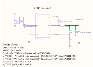
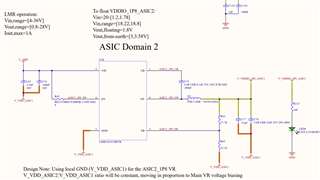
I'm using the LMR54410 in my design, which has a floating ground (aka localGND, also called "V_VDD_ASIC1" in the schematic). 

My intended design:

Vin=20VDC* (18.5V from localGND)

Vout=3.3VDC* (1.8V from localGND)

*in reference to Earth GND

Note: my localGND varies but should be 1.5V* nominal.

I am measuring localGND at 1.2V*. This is an acceptable localGND voltage with respect to my application.

I measure a steady 20V* input, but I measure the output consistently low, ~2.2V*. (i.e. only 1V higher than the localGND).

Can you please review the schematic and offer any comments regarding why I am seeing the wrong output voltage, whether it is related to the localGND or some other issue?

Thanks,

Tom

  • Hi Tom,

    Correct me if I am wrong, let's say that V_VDD_ASIC1 is at 0V and looking at your schematic, I see that resistor divider will set the output voltage to yield 1.8V, right? Therefore, if V_VDD_ASIC1 is measured to be 1.2V, which is what you are measuring in respect to PE GND, the actual output voltage should be 3V, but you are measuring only 2.2V from respect to PE GND.

    Can you provide a scope shot of the SW node, CB, VIN and VOUT? What is the load that you are applying to the IC?

    Ben

  • Hi Tom,

    Are there any updates?

    Ben

  • Hi Ben,

    Thanks for taking a look.

    In fact, I do have this same circuit duplicated on the board with a PE GND reference (image below, U18). It does yield the desired 1.8V.

    Correct, the output voltage on U20 should be 3V and I'm measuring 2.2V. I still need to take the scope captures.

    My load includes two ASIC chips "stacked" vertically. The ASICs have 3 power rails--1.5V (aka "VDDC" the core voltage),1.8V (VCCIO), and 0.8V (VCCANA), with the most current draw being on 1.5V. ASIC 1 GND reference is Earth (PE GND), and ASIC 2 GND reference is 1.5V (This is why I say they are stacked, the GND of one ASIC becomes the VDDC of the lower ASIC). As a model, these ASICs act as a resistive load with very low resistance (~1 Ohm) between VDDC and GND. Sidenote: I also have the 0.8V LDO (ADP171) coming off the 1.8V LMR54410.

    This ASIC "stacking" may appear novel but it is common in my application, with other VRs successfully working. Since we know the LMR is working with a traditional PE GND, I'm wondering how I may have "upset" the circuit with this floating GND and what goes on inside the LMR that may make it incompatible with my circuit, e.g. possibly the feedback node?

    Thanks,

    Tom

  • Hi Tom,

    Have you tried setting up each reference rail to PE GND to check if the whole schematic is working? Just want to make sure the BOM components are not the issue. I would check each regulator and then start stacking each regulator. 

    The one concern I have is when the second stack converter is in the synchronous mode, what is the first converter doing with the current of the second inductor? Is the current sinking to PE GND by the first converter? I think the converters need to have its own isolation to PE GND. 

    Ben

  • Hi Tom,

    Are there any new updates?

    Ben

  • Hi Tom,

    If there are no additional questions and my answer above satisfies your question, please close the thread by clicking on "resolved". Thanks,

    Ben